

Viz Specifikace pro podrobnosti o produktu.
MAX16126TCD/V+T
Product Overview
- Category: Integrated Circuit (IC)
- Use: Power Management
- Characteristics: High Efficiency, Low Quiescent Current, Wide Input Voltage Range
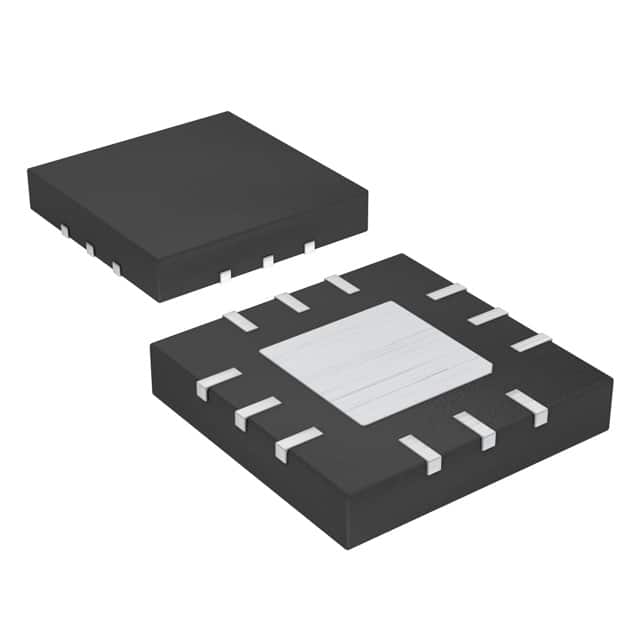
- Package: TDFN-8 (3mm x 3mm)
- Essence: Voltage Regulator
- Packaging/Quantity: Tape and Reel, 2500 units per reel
Specifications
- Input Voltage Range: 4.5V to 60V
- Output Voltage Range: 0.6V to 0.9 x VIN
- Output Current: Up to 1A
- Quiescent Current: 17µA (typical)
- Switching Frequency: 500kHz (typical)
- Operating Temperature Range: -40°C to +125°C
Detailed Pin Configuration
The MAX16126TCD/V+T has the following pin configuration:
- GND: Ground connection
- EN: Enable pin for turning the regulator on/off
- FB: Feedback pin for setting the output voltage
- SW: Switching node for connecting the inductor
- LX: Inductor connection
- PGND: Power ground connection
- VCC: Supply voltage input
- VIN: Input voltage connection
Functional Features
- High efficiency synchronous buck regulator
- Integrated low RDS(ON) high-side and low-side MOSFETs
- Adjustable output voltage through external resistors
- Soft-start feature for controlled startup
- Overcurrent protection and thermal shutdown
- Under-voltage lockout (UVLO) protection
Advantages and Disadvantages
Advantages
- Wide input voltage range allows for versatile applications
- High efficiency results in reduced power dissipation
- Low quiescent current minimizes standby power consumption
- Compact package size enables space-constrained designs
Disadvantages
- Limited output current may not be suitable for high-power applications
- Requires external components for proper operation
- Higher cost compared to non-integrated voltage regulators
Working Principles
The MAX16126TCD/V+T is a synchronous buck regulator that converts a higher input voltage to a lower output voltage. It utilizes high-side and low-side MOSFETs to efficiently regulate the output voltage. The feedback pin (FB) allows the user to set the desired output voltage by connecting external resistors. The enable pin (EN) controls the on/off state of the regulator.
During operation, the regulator continuously switches the high-side and low-side MOSFETs to control the energy flow from the input to the output. This switching action, along with the inductor and capacitors, helps maintain a stable output voltage. The soft-start feature ensures a controlled startup, preventing excessive inrush current.
The MAX16126TCD/V+T also incorporates various protection features such as overcurrent protection, thermal shutdown, and under-voltage lockout (UVLO). These safeguards help protect the regulator and the connected circuitry from damage during fault conditions.
Detailed Application Field Plans
The MAX16126TCD/V+T can be used in various applications, including:
- Automotive: Power management in automotive systems, such as infotainment systems, lighting, and motor control.
- Industrial: Voltage regulation in industrial automation, robotics, and control systems.
- Telecommunications: Power supply for telecom infrastructure equipment, base stations, and network devices.
- Consumer Electronics: Voltage regulation in portable devices, home appliances, and audio/video equipment.
- IoT and Wearables: Power management in Internet of Things (IoT) devices, wearables, and smart home applications.
Detailed and Complete Alternative Models
- MAX16127TCD/V+T: Similar specifications, but with higher output current capability (up to 2A).
- MAX16128TCD/V+T: Higher input voltage range (up to 72V) and adjustable switching frequency.
- MAX16129TCD/V+T: Lower quiescent current (10µA typical) for ultra-low power applications.
These alternative models offer similar functionality and can be considered based on specific requirements and design constraints.
Word count: 525 words
Seznam 10 běžných otázek a odpovědí souvisejících s aplikací MAX16126TCD/V+T v technických řešeních
Question: What is the maximum input voltage for MAX16126TCD/V+T?
Answer: The maximum input voltage for MAX16126TCD/V+T is 28V.Question: What is the typical quiescent current of MAX16126TCD/V+T?
Answer: The typical quiescent current of MAX16126TCD/V+T is 15µA.Question: Can MAX16126TCD/V+T be used in automotive applications?
Answer: Yes, MAX16126TCD/V+T is suitable for automotive applications.Question: What is the output current capability of MAX16126TCD/V+T?
Answer: MAX16126TCD/V+T can provide up to 300mA of output current.Question: Is MAX16126TCD/V+T suitable for battery-powered applications?
Answer: Yes, MAX16126TCD/V+T is well-suited for battery-powered applications.Question: What is the operating temperature range of MAX16126TCD/V+T?
Answer: MAX16126TCD/V+T can operate within a temperature range of -40°C to +125°C.Question: Does MAX16126TCD/V+T have built-in overcurrent protection?
Answer: Yes, MAX16126TCD/V+T features built-in overcurrent protection.Question: Can MAX16126TCD/V+T be used in industrial control systems?
Answer: Yes, MAX16126TCD/V+T is suitable for use in industrial control systems.Question: What is the package type of MAX16126TCD/V+T?
Answer: MAX16126TCD/V+T is available in a 6-pin TDFN package.Question: Does MAX16126TCD/V+T require external compensation components?
Answer: No, MAX16126TCD/V+T does not require external compensation components.