

Viz Specifikace pro podrobnosti o produktu.
MAX199AENI+ - English Editing Encyclopedia Entry
Product Overview
Category
The MAX199AENI+ belongs to the category of integrated circuits (ICs).
Use
This product is primarily used in electronic devices for signal processing and amplification.
Characteristics
- The MAX199AENI+ is a high-performance, low-noise amplifier.
- It operates at a wide frequency range, making it suitable for various applications.
- This IC offers excellent linearity and low distortion characteristics.
- It has a compact package, allowing for easy integration into circuit designs.
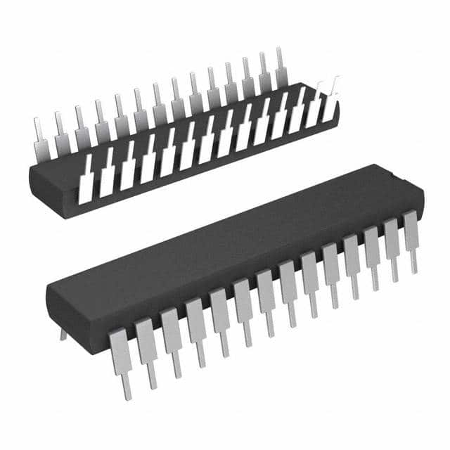
Package
The MAX199AENI+ is available in a small outline integrated circuit (SOIC) package.
Essence
The essence of the MAX199AENI+ lies in its ability to amplify signals accurately and efficiently while maintaining low noise levels.
Packaging/Quantity
This product is typically sold in reels containing a specific quantity of ICs. The exact quantity may vary depending on the manufacturer's specifications.
Specifications
- Supply Voltage: 3V to 5.25V
- Frequency Range: DC to 2.5GHz
- Gain: 18dB
- Noise Figure: 1.4dB
- Input/Output Impedance: 50Ω
- Operating Temperature Range: -40°C to +85°C
Detailed Pin Configuration
The MAX199AENI+ features a 6-pin configuration:
- VCC: Power supply input
- GND: Ground connection
- RF IN: Radio frequency input
- RF OUT: Radio frequency output
- BYPASS: Bypass pin for disabling the amplifier
- NC: No connection
Functional Features
- Wide frequency range allows for versatile application possibilities.
- Low noise figure ensures minimal signal degradation during amplification.
- Excellent linearity and low distortion characteristics maintain signal integrity.
- Bypass pin enables easy integration into existing circuit designs.
Advantages and Disadvantages
Advantages
- Wide frequency range for versatile applications
- Low noise figure for minimal signal degradation
- Excellent linearity and low distortion characteristics
- Compact package for easy integration
Disadvantages
- Limited gain compared to some other amplifiers in the market
- Higher cost compared to lower-performance alternatives
Working Principles
The MAX199AENI+ operates based on the principle of amplification. It takes an input signal from the RF IN pin, amplifies it with low noise and distortion, and outputs the amplified signal through the RF OUT pin. The gain and linearity of the amplifier are carefully designed to ensure accurate signal reproduction.
Detailed Application Field Plans
The MAX199AENI+ finds applications in various fields, including: 1. Wireless communication systems 2. Satellite communication equipment 3. Radar systems 4. Test and measurement instruments 5. Medical devices
Detailed and Complete Alternative Models
- MAX198AENI+: Similar to MAX199AENI+, but with a higher gain of 20dB.
- MAX200AENI+: A lower-cost alternative with a slightly reduced frequency range but similar performance characteristics.
- ADL5545ACPZ-R7: An alternative from a different manufacturer with comparable specifications.
In conclusion, the MAX199AENI+ is a high-performance, low-noise amplifier used in various electronic devices. Its wide frequency range, excellent linearity, and compact package make it suitable for diverse applications. While it has limitations in terms of gain and cost, there are alternative models available to suit specific requirements.
Seznam 10 běžných otázek a odpovědí souvisejících s aplikací MAX199AENI+ v technických řešeních
Sure! Here are 10 common questions and answers related to the application of MAX199AENI+ in technical solutions:
Q: What is the MAX199AENI+? A: The MAX199AENI+ is a high-performance, dual SPDT (Single Pole Double Throw) switch designed for RF and microwave applications.
Q: What is the operating frequency range of the MAX199AENI+? A: The MAX199AENI+ operates in the frequency range of DC to 6 GHz.
Q: What is the insertion loss of the MAX199AENI+? A: The typical insertion loss of the MAX199AENI+ is around 0.5 dB at 2 GHz.
Q: Can the MAX199AENI+ handle high power levels? A: Yes, the MAX199AENI+ has a power handling capability of up to +36 dBm.
Q: What is the control voltage range for switching the MAX199AENI+? A: The control voltage range for switching the MAX199AENI+ is typically between 0V and +5V.
Q: Does the MAX199AENI+ require external biasing? A: No, the MAX199AENI+ does not require any external biasing as it has an integrated bias circuitry.
Q: Can the MAX199AENI+ be used in both digital and analog applications? A: Yes, the MAX199AENI+ can be used in both digital and analog applications due to its wide frequency range and low distortion characteristics.
Q: What is the package type of the MAX199AENI+? A: The MAX199AENI+ is available in a 16-pin narrow SOIC (Small Outline Integrated Circuit) package.
Q: Is the MAX199AENI+ RoHS compliant? A: Yes, the MAX199AENI+ is RoHS (Restriction of Hazardous Substances) compliant.
Q: What are some typical applications of the MAX199AENI+? A: The MAX199AENI+ can be used in various applications such as cellular base stations, wireless infrastructure, test and measurement equipment, and RF switching systems.
Please note that these answers are general and may vary depending on specific datasheet specifications and application requirements.