

Viz Specifikace pro podrobnosti o produktu.
MAX5732BUTN+ - English Editing Encyclopedia Entry
Product Overview
Category
MAX5732BUTN+ belongs to the category of integrated circuits (ICs).
Use
This product is commonly used in electronic devices for digital-to-analog conversion.
Characteristics
- High precision and accuracy
- Low power consumption
- Wide operating voltage range
- Compact package size
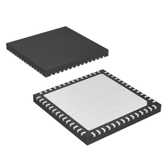
Package
The MAX5732BUTN+ is available in a small outline transistor (SOT) package.
Essence
The essence of MAX5732BUTN+ lies in its ability to convert digital signals into analog voltages with high precision and efficiency.
Packaging/Quantity
This product is typically packaged in reels, with a quantity of 2500 units per reel.
Specifications
- Resolution: 12 bits
- Supply Voltage Range: 2.7V to 5.5V
- Operating Temperature Range: -40°C to +85°C
- Output Voltage Range: 0V to Vref
- DNL (Differential Non-Linearity): ±0.5 LSB (max)
- INL (Integral Non-Linearity): ±1 LSB (max)
Detailed Pin Configuration
The MAX5732BUTN+ has the following pin configuration:
- VDD - Power supply input
- GND - Ground reference
- DIN - Digital input for data transfer
- CS - Chip select input
- SCLK - Serial clock input
- LDAC - Load DAC input
- REF - Reference voltage input
- OUT - Analog output
Functional Features
- Serial interface for easy integration with microcontrollers
- On-chip voltage reference for accurate conversions
- Power-down mode for reduced power consumption
- Fast settling time for rapid response
Advantages and Disadvantages
Advantages
- High precision and accuracy in digital-to-analog conversion
- Wide operating voltage range allows for versatile applications
- Compact package size enables space-saving designs
- Low power consumption for energy-efficient devices
Disadvantages
- Limited resolution compared to higher-end DACs
- May require additional external components for specific applications
Working Principles
The MAX5732BUTN+ utilizes a digital-to-analog converter (DAC) architecture to convert binary digital signals into corresponding analog voltages. It employs an internal reference voltage to achieve high precision and accuracy in the conversion process. The serial interface allows for easy integration with microcontrollers, enabling seamless communication and control.
Detailed Application Field Plans
The MAX5732BUTN+ finds applications in various fields, including: 1. Audio equipment 2. Industrial automation 3. Test and measurement instruments 4. Communication systems 5. Automotive electronics
Detailed and Complete Alternative Models
Some alternative models that offer similar functionality to the MAX5732BUTN+ include: 1. LTC1661 - 12-Bit Serial DAC 2. MCP4921 - Single Channel 12-Bit DAC 3. AD5620 - 12-Bit nanoDAC
These alternative models provide comparable features and can be considered as substitutes based on specific application requirements.
In conclusion, the MAX5732BUTN+ is a highly precise and efficient digital-to-analog converter integrated circuit. Its compact size, wide operating voltage range, and low power consumption make it suitable for various applications in different industries. While it may have limitations in terms of resolution and additional external component requirements, alternative models are available to cater to specific needs.
Seznam 10 běžných otázek a odpovědí souvisejících s aplikací MAX5732BUTN+ v technických řešeních
Sure! Here are 10 common questions and answers related to the application of MAX5732BUTN+ in technical solutions:
Q: What is the MAX5732BUTN+? A: The MAX5732BUTN+ is a high-speed, low-power, 16-bit digital-to-analog converter (DAC) with an integrated output amplifier.
Q: What is the operating voltage range of the MAX5732BUTN+? A: The operating voltage range of the MAX5732BUTN+ is from 2.7V to 5.5V.
Q: What is the maximum output current of the MAX5732BUTN+? A: The maximum output current of the MAX5732BUTN+ is ±20mA.
Q: Can the MAX5732BUTN+ be used in both single-ended and differential output configurations? A: Yes, the MAX5732BUTN+ can be used in both single-ended and differential output configurations.
Q: What is the settling time of the MAX5732BUTN+? A: The settling time of the MAX5732BUTN+ is typically 8µs for a full-scale step.
Q: Does the MAX5732BUTN+ have a power-on reset feature? A: Yes, the MAX5732BUTN+ has a power-on reset feature that ensures the DAC outputs are at zero-scale on power-up.
Q: Can the MAX5732BUTN+ operate in a temperature range outside the industrial range? A: No, the MAX5732BUTN+ is designed to operate within the industrial temperature range of -40°C to +85°C.
Q: What is the resolution of the MAX5732BUTN+? A: The MAX5732BUTN+ has a resolution of 16 bits, allowing for 65,536 possible output levels.
Q: Does the MAX5732BUTN+ have any integrated protection features? A: Yes, the MAX5732BUTN+ includes integrated thermal shutdown and short-circuit protection features.
Q: Can the MAX5732BUTN+ be controlled using a serial interface? A: Yes, the MAX5732BUTN+ can be controlled using a standard SPI (Serial Peripheral Interface) interface.
Please note that these answers are general and may vary depending on the specific application and requirements. It is always recommended to refer to the datasheet and application notes for detailed information.