

Viz Specifikace pro podrobnosti o produktu.
MAX8685FETD+ - English Editing Encyclopedia Entry
Product Overview
Category
MAX8685FETD+ belongs to the category of integrated circuits (ICs).
Use
This product is commonly used in electronic devices for voltage regulation and power management.
Characteristics
- Voltage regulation and power management capabilities
- High efficiency
- Compact size
- Wide input voltage range
- Low power consumption
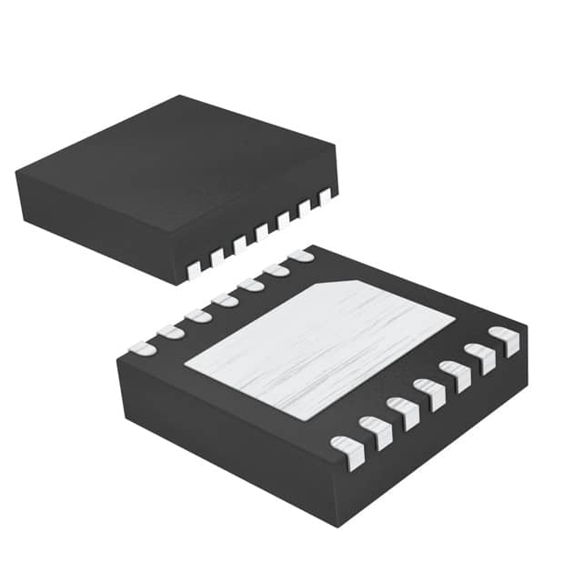
Package
The MAX8685FETD+ is available in a small form factor package, allowing for easy integration into various electronic devices.
Essence
The essence of MAX8685FETD+ lies in its ability to efficiently regulate voltage and manage power consumption in electronic devices.
Packaging/Quantity
This product is typically packaged in reels or tubes, with a quantity of 250 units per reel/tube.
Specifications
- Input Voltage Range: 4.5V to 28V
- Output Voltage Range: 0.8V to 5.5V
- Maximum Output Current: 3A
- Efficiency: Up to 95%
- Operating Temperature Range: -40°C to +85°C
Detailed Pin Configuration
The MAX8685FETD+ has the following pin configuration:
- VIN: Input voltage pin
- GND: Ground pin
- EN: Enable pin
- FB: Feedback pin
- VOUT: Output voltage pin
Functional Features
- Wide input voltage range allows for compatibility with various power sources.
- High efficiency ensures minimal power loss during voltage regulation.
- Compact size enables integration into space-constrained electronic devices.
- Enable pin provides control over the device's operation.
- Feedback pin allows for precise voltage regulation.
Advantages and Disadvantages
Advantages
- High efficiency results in reduced power consumption.
- Wide input voltage range enhances versatility.
- Compact size facilitates integration into small devices.
- Precise voltage regulation ensures stable performance.
Disadvantages
- Limited maximum output current may not be suitable for high-power applications.
- Operating temperature range may restrict usage in extreme environments.
Working Principles
The MAX8685FETD+ utilizes advanced voltage regulation techniques to maintain a stable output voltage. It employs a feedback mechanism to continuously monitor the output voltage and adjust it accordingly. By efficiently converting the input voltage to the desired output voltage, this device ensures optimal power management.
Detailed Application Field Plans
The MAX8685FETD+ finds applications in various electronic devices, including but not limited to: - Mobile phones - Tablets - Portable gaming consoles - IoT devices - Automotive electronics - Industrial equipment
Detailed and Complete Alternative Models
- MAX8686FETD+: Similar to MAX8685FETD+, but with a higher maximum output current of 5A.
- MAX8684FETD+: Similar to MAX8685FETD+, but with a lower maximum output current of 2A.
- MAX8687FETD+: Similar to MAX8685FETD+, but with additional features such as overvoltage protection and thermal shutdown.
These alternative models provide options with varying specifications to suit different application requirements.
In conclusion, the MAX8685FETD+ is an integrated circuit that offers efficient voltage regulation and power management capabilities. Its compact size, wide input voltage range, and high efficiency make it suitable for a range of electronic devices. While it has limitations in terms of maximum output current and operating temperature range, alternative models are available to address specific needs.
Seznam 10 běžných otázek a odpovědí souvisejících s aplikací MAX8685FETD+ v technických řešeních
Sure! Here are 10 common questions and answers related to the application of MAX8685FETD+ in technical solutions:
Q: What is the MAX8685FETD+? A: The MAX8685FETD+ is a high-efficiency, synchronous step-down DC-DC converter with integrated MOSFETs.
Q: What is the input voltage range of the MAX8685FETD+? A: The input voltage range of the MAX8685FETD+ is typically between 4.5V and 28V.
Q: What is the output voltage range of the MAX8685FETD+? A: The output voltage range of the MAX8685FETD+ can be programmed from 0.6V to 90% of the input voltage.
Q: What is the maximum output current of the MAX8685FETD+? A: The maximum output current of the MAX8685FETD+ is typically 3A.
Q: Does the MAX8685FETD+ have built-in protection features? A: Yes, the MAX8685FETD+ includes overcurrent protection, thermal shutdown, and undervoltage lockout.
Q: Can the MAX8685FETD+ operate in a wide temperature range? A: Yes, the MAX8685FETD+ is designed to operate in a temperature range of -40°C to +125°C.
Q: Is the MAX8685FETD+ suitable for battery-powered applications? A: Yes, the MAX8685FETD+ is suitable for battery-powered applications due to its low quiescent current and high efficiency.
Q: Can the MAX8685FETD+ be used in automotive applications? A: Yes, the MAX8685FETD+ is automotive-grade and can be used in automotive applications.
Q: Does the MAX8685FETD+ require external compensation components? A: No, the MAX8685FETD+ has an internal compensation network, eliminating the need for external components.
Q: What package options are available for the MAX8685FETD+? A: The MAX8685FETD+ is available in a 16-pin TDFN package and a 16-pin QSOP package.
Please note that these answers are general and may vary depending on the specific datasheet and application requirements.