

Viz Specifikace pro podrobnosti o produktu.
ATF1504AS-10JC44
Product Overview
Category
ATF1504AS-10JC44 belongs to the category of programmable logic devices (PLDs).
Use
This product is commonly used in digital circuit design and implementation. It provides a flexible and customizable solution for various applications.
Characteristics
- Programmable: The ATF1504AS-10JC44 can be programmed to perform specific functions according to the user's requirements.
- High Integration: It integrates multiple logic gates, flip-flops, and other components into a single device, reducing the need for external components.
- Versatile: It supports a wide range of applications due to its programmability.
- Compact Package: The ATF1504AS-10JC44 comes in a small package, making it suitable for space-constrained designs.
- Low Power Consumption: This device operates at low power, making it energy-efficient.
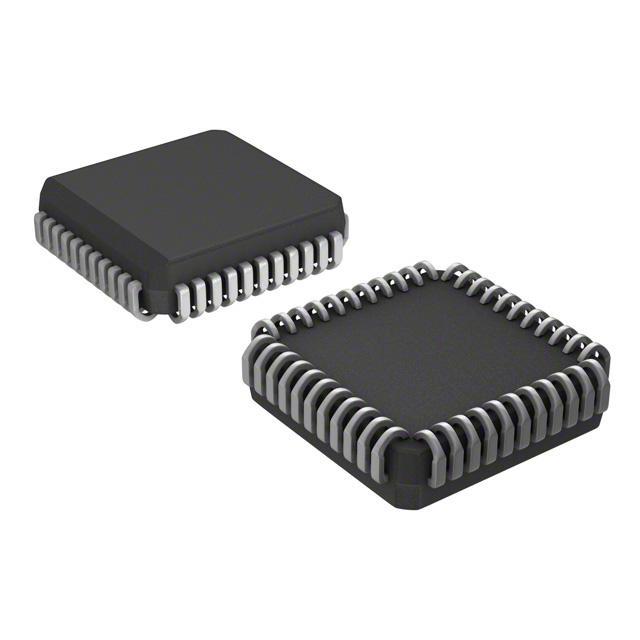
Package and Quantity
The ATF1504AS-10JC44 is available in a 44-pin PLCC (Plastic Leaded Chip Carrier) package. Each package contains one unit of the device.
Specifications
- Device Type: ATF1504AS-10JC44
- Logic Cells: 1504
- I/O Pins: 36
- Operating Voltage: 3.3V
- Speed Grade: -10
- Maximum Frequency: 100 MHz
- Programming Technology: In-System Programmable (ISP)
- Package Type: PLCC-44
Pin Configuration
The ATF1504AS-10JC44 has a total of 44 pins. Here is the detailed pin configuration:
(Pin Number - Pin Name - Description)
1 - VCCIO - I/O Supply Voltage 2 - GND - Ground 3 - TCK - Test Clock Input 4 - TDI - Test Data Input 5 - TDO - Test Data Output 6 - TMS - Test Mode Select 7 - VCC - Power Supply Voltage 8 - GND - Ground 9 - I/O0 - General Purpose I/O Pin 0 10 - I/O1 - General Purpose I/O Pin 1 11 - I/O2 - General Purpose I/O Pin 2 12 - I/O3 - General Purpose I/O Pin 3 13 - I/O4 - General Purpose I/O Pin 4 14 - I/O5 - General Purpose I/O Pin 5 15 - I/O6 - General Purpose I/O Pin 6 16 - I/O7 - General Purpose I/O Pin 7 17 - I/O8 - General Purpose I/O Pin 8 18 - I/O9 - General Purpose I/O Pin 9 19 - I/O10 - General Purpose I/O Pin 10 20 - I/O11 - General Purpose I/O Pin 11 21 - I/O12 - General Purpose I/O Pin 12 22 - I/O13 - General Purpose I/O Pin 13 23 - I/O14 - General Purpose I/O Pin 14 24 - I/O15 - General Purpose I/O Pin 15 25 - I/O16 - General Purpose I/O Pin 16 26 - I/O17 - General Purpose I/O Pin 17 27 - I/O18 - General Purpose I/O Pin 18 28 - I/O19 - General Purpose I/O Pin 19 29 - I/O20 - General Purpose I/O Pin 20 30 - I/O21 - General Purpose I/O Pin 21 31 - I/O22 - General Purpose I/O Pin 22 32 - I/O23 - General Purpose I/O Pin 23 33 - I/O24 - General Purpose I/O Pin 24 34 - I/O25 - General Purpose I/O Pin 25 35 - I/O26 - General Purpose I/O Pin 26 36 - I/O27 - General Purpose I/O Pin 27 37 - I/O28 - General Purpose I/O Pin 28 38 - I/O29 - General Purpose I/O Pin 29 39 - I/O30 - General Purpose I/O Pin 30 40 - I/O31 - General Purpose I/O Pin 31 41 - I/O32 - General Purpose I/O Pin 32 42 - I/O33 - General Purpose I/O Pin 33 43 - I/O34 - General Purpose I/O Pin 34 44 - I/O35 - General Purpose I/O Pin 35
Functional Features
- Programmability: The ATF1504AS-10JC44 can be programmed to implement various logic functions, allowing for customization and flexibility in circuit design.
- High Integration: With 1504 logic cells, this device offers a high level of integration, reducing the need for additional components.
- In-System Programmable (ISP): The ATF1504AS-10JC44 supports in-system
Seznam 10 běžných otázek a odpovědí souvisejících s aplikací ATF1504AS-10JC44 v technických řešeních
Sure! Here are 10 common questions and answers related to the application of ATF1504AS-10JC44 in technical solutions:
Q: What is ATF1504AS-10JC44? A: ATF1504AS-10JC44 is a specific model of Field-Programmable Gate Array (FPGA) manufactured by Microchip Technology Inc.
Q: What are the key features of ATF1504AS-10JC44? A: Some key features of ATF1504AS-10JC44 include 1500 usable gates, 44-pin PLCC package, 10ns maximum propagation delay, and 5V operation.
Q: What are the typical applications of ATF1504AS-10JC44? A: ATF1504AS-10JC44 is commonly used in various technical solutions such as industrial control systems, communication equipment, medical devices, and automotive electronics.
Q: How can I program ATF1504AS-10JC44? A: ATF1504AS-10JC44 can be programmed using industry-standard hardware description languages (HDLs) like VHDL or Verilog, along with appropriate programming tools provided by the manufacturer.
Q: Can ATF1504AS-10JC44 be reprogrammed after initial programming? A: No, ATF1504AS-10JC44 is a one-time programmable (OTP) FPGA, meaning it cannot be reprogrammed once it has been programmed.
Q: What voltage level does ATF1504AS-10JC44 operate at? A: ATF1504AS-10JC44 operates at a voltage level of 5V.
Q: Is ATF1504AS-10JC44 suitable for low-power applications? A: No, ATF1504AS-10JC44 is not specifically designed for low-power applications. It is more suitable for applications where higher performance and functionality are required.
Q: Can ATF1504AS-10JC44 interface with other digital components? A: Yes, ATF1504AS-10JC44 can interface with other digital components such as microcontrollers, memory devices, sensors, and communication interfaces using standard protocols like SPI or I2C.
Q: What is the maximum clock frequency supported by ATF1504AS-10JC44? A: The maximum clock frequency supported by ATF1504AS-10JC44 is dependent on the specific design and implementation, but it can typically operate at frequencies up to 50 MHz.
Q: Are there any specific design considerations when using ATF1504AS-10JC44? A: Yes, some design considerations include power supply decoupling, signal integrity, thermal management, and proper grounding techniques to ensure reliable operation of ATF1504AS-10JC44 in the intended application.
Please note that these answers are general and may vary depending on the specific requirements and context of your technical solution.