

Viz Specifikace pro podrobnosti o produktu.
ATF1504ASV-15JI44
Product Overview
Category
ATF1504ASV-15JI44 belongs to the category of programmable logic devices (PLDs).
Use
This product is primarily used in digital circuit design and implementation. It provides a flexible and customizable solution for various applications.
Characteristics
- Programmable: The ATF1504ASV-15JI44 can be programmed to perform specific functions based on user requirements.
- High Integration: It offers a high level of integration, allowing multiple logic functions to be implemented within a single device.
- Versatile: This PLD supports a wide range of applications, making it suitable for diverse industries.
- Compact Package: The ATF1504ASV-15JI44 comes in a small package, which makes it ideal for space-constrained designs.
- Low Power Consumption: It operates at low power levels, ensuring energy efficiency.
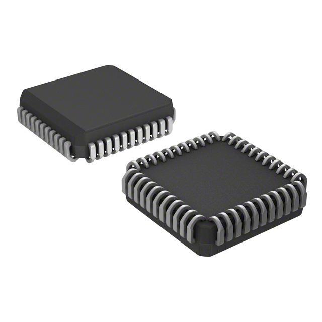
Package and Quantity
The ATF1504ASV-15JI44 is available in a 44-pin plastic quad flat pack (PQFP) package. Each package contains one unit of the device.
Specifications
- Device Type: Programmable Logic Device (PLD)
- Family: ATF1504ASV
- Speed Grade: 15
- Package Type: 44-pin PQFP
- Operating Voltage: 3.3V
- Maximum Operating Frequency: 100 MHz
- Number of Logic Elements: 1504
- Number of Input/Output Pins: 36
- Programmable Gates: 4000
- On-Chip Memory: 64K bits
- JTAG Support: Yes
Detailed Pin Configuration
The ATF1504ASV-15JI44 has a total of 44 pins. Here is a detailed pin configuration:
- VCCIO
- GND
- I/O_0
- I/O_1
- I/O_2
- I/O_3
- I/O_4
- I/O_5
- I/O_6
- I/O_7
- I/O_8
- I/O_9
- I/O_10
- I/O_11
- I/O_12
- I/O_13
- I/O_14
- I/O_15
- I/O_16
- I/O_17
- I/O_18
- I/O_19
- I/O_20
- I/O_21
- I/O_22
- I/O_23
- I/O_24
- I/O_25
- I/O_26
- I/O_27
- I/O_28
- I/O_29
- I/O_30
- I/O_31
- I/O_32
- I/O_33
- I/O_34
- I/O_35
- TCK
- TMS
- TDI
- TDO
- GND
- VCC
Functional Features
- Flexible Logic Configuration: The ATF1504ASV-15JI44 allows users to configure the logic functions according to their specific requirements.
- In-System Programming (ISP): This PLD supports ISP, enabling users to program or reprogram the device while it is in the target system.
- JTAG Boundary Scan: The built-in JTAG support facilitates boundary scan testing and debugging of the device.
- High-Speed Operation: With a maximum operating frequency of 100 MHz, the ATF1504ASV-15JI44 can handle complex digital circuits efficiently.
Advantages and Disadvantages
Advantages
- Customizability: The ATF1504ASV-15JI44 offers a high degree of customization, allowing users to tailor the logic functions to their specific needs.
- Integration: With its high integration level, this PLD eliminates the need for multiple discrete components, reducing overall system complexity.
- Space Efficiency: The compact package of the ATF1504ASV-15JI44 makes it suitable for designs with limited space.
- Energy Efficiency: Operating at low power levels, this device ensures energy-efficient operation.
Disadvantages
- Learning Curve: Utilizing the full potential of the ATF1504ASV-15JI44 may require a learning curve, especially for users new to programmable logic devices.
- Limited I/O Pins: The device has a limited number of input/output pins, which may restrict the complexity of certain designs.
Working Principles
The ATF1504ASV-15JI44 operates based on the principles of programmable logic. It consists of configurable logic blocks (CLBs), interconnect resources, and input/output
Seznam 10 běžných otázek a odpovědí souvisejících s aplikací ATF1504ASV-15JI44 v technických řešeních
Sure! Here are 10 common questions and answers related to the application of ATF1504ASV-15JI44 in technical solutions:
Q: What is ATF1504ASV-15JI44? A: ATF1504ASV-15JI44 is a specific model of Field-Programmable Gate Array (FPGA) manufactured by Microchip Technology.
Q: What are the key features of ATF1504ASV-15JI44? A: Some key features of ATF1504ASV-15JI44 include 1500 usable gates, 44-pin PLCC package, 15ns maximum propagation delay, and 5V voltage compatibility.
Q: How can ATF1504ASV-15JI44 be used in technical solutions? A: ATF1504ASV-15JI44 can be used for various applications such as digital logic design, prototyping, system integration, and hardware acceleration.
Q: What programming language is used to configure ATF1504ASV-15JI44? A: ATF1504ASV-15JI44 can be configured using Hardware Description Languages (HDLs) like VHDL or Verilog.
Q: Can ATF1504ASV-15JI44 be reprogrammed after configuration? A: No, ATF1504ASV-15JI44 is a one-time programmable FPGA and cannot be reprogrammed once it has been configured.
Q: What tools are required to program ATF1504ASV-15JI44? A: To program ATF1504ASV-15JI44, you will need a compatible programmer device, such as a USB Blaster or ByteBlaster, along with the appropriate software provided by the manufacturer.
Q: What is the power supply requirement for ATF1504ASV-15JI44? A: ATF1504ASV-15JI44 operates on a 5V power supply, so it requires a stable 5V DC power source.
Q: Can ATF1504ASV-15JI44 interface with other components or devices? A: Yes, ATF1504ASV-15JI44 can interface with other components and devices through its I/O pins, allowing communication and integration with external systems.
Q: Are there any limitations to using ATF1504ASV-15JI44 in technical solutions? A: Some limitations include limited gate count, lack of reprogrammability, and potential compatibility issues with newer technologies due to its older design.
Q: Where can I find more information about ATF1504ASV-15JI44 and its application in technical solutions? A: You can refer to the manufacturer's datasheet, application notes, or online forums dedicated to FPGA programming and applications for more detailed information and guidance.