

Viz Specifikace pro podrobnosti o produktu.
ATF1508BE-5AX100
Product Overview
Category
ATF1508BE-5AX100 belongs to the category of programmable logic devices (PLDs).
Use
This product is commonly used in digital circuit design and implementation. It provides a flexible and customizable solution for various applications.
Characteristics
- Programmable: The ATF1508BE-5AX100 can be programmed to perform specific functions according to the user's requirements.
- High Integration: It integrates multiple logic gates, flip-flops, and other components into a single device, reducing the need for external components.
- Versatile: This PLD can be used in a wide range of applications, including telecommunications, automotive, industrial control, and consumer electronics.
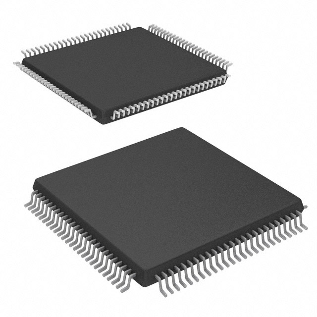
Package
The ATF1508BE-5AX100 is available in a 100-pin TQFP (Thin Quad Flat Pack) package.
Essence
The essence of ATF1508BE-5AX100 lies in its ability to provide reconfigurable logic functions, allowing designers to implement complex digital circuits efficiently.
Packaging/Quantity
This product is typically packaged in reels or trays, with a quantity of 250 units per reel/tray.
Specifications
- Technology: CMOS
- Number of Logic Cells: 1,500
- Maximum Operating Frequency: 100 MHz
- Operating Voltage: 3.3V
- I/O Pins: 80
- Programmable Logic Blocks: 48
- Macrocells: 1,200
- On-Chip Memory: 16 Kbits
- JTAG Boundary Scan Support: Yes
Detailed Pin Configuration
The ATF1508BE-5AX100 has a total of 100 pins. Here is a detailed pin configuration:
(Pin Number - Pin Name - Description) 1 - VCCIO - I/O Power Supply 2 - GND - Ground 3 - TDI - Test Data Input 4 - TMS - Test Mode Select 5 - TCK - Test Clock 6 - TDO - Test Data Output 7 - VCC - Power Supply 8 - GND - Ground 9 - NC - No Connect 10 - I/O0 - General Purpose I/O Pin 0 11 - I/O1 - General Purpose I/O Pin 1 ... 100 - I/O79 - General Purpose I/O Pin 79
Functional Features
- Reconfigurable Logic: The ATF1508BE-5AX100 can be programmed to implement various logic functions, allowing for flexibility in circuit design.
- High-Speed Operation: With a maximum operating frequency of 100 MHz, this PLD can handle complex digital operations efficiently.
- JTAG Boundary Scan Support: The built-in JTAG support enables easy testing and debugging of the device during development and production stages.
Advantages and Disadvantages
Advantages
- Flexibility: The reprogrammable nature of ATF1508BE-5AX100 allows for quick design iterations and modifications.
- Integration: This PLD integrates multiple components into a single device, reducing the need for external components and saving board space.
- Cost-Effective: By eliminating the need for custom-designed ASICs, the ATF1508BE-5AX100 offers a cost-effective solution for digital circuit implementation.
Disadvantages
- Limited Complexity: While versatile, the ATF1508BE-5AX100 has a finite number of logic cells and macrocells, which may limit its ability to handle extremely complex designs.
- Programming Overhead: Programming the device requires specialized tools and knowledge, adding an extra step to the design process.
Working Principles
The ATF1508BE-5AX100 utilizes a combination of programmable logic blocks, interconnect resources, and on-chip memory to implement user-defined logic functions. The device is programmed using a hardware description language (HDL) or a graphical design tool, which generates a configuration file. This file is then loaded onto the ATF1508BE-5AX100, configuring it to perform the desired logic operations.
Detailed Application Field Plans
The ATF1508BE-5AX100 finds applications in various fields, including:
- Telecommunications: Used in network routers, switches, and communication equipment for signal processing and protocol handling.
- Automotive: Employed in automotive electronics for engine control units, dashboard displays, and safety systems.
- Industrial Control: Utilized in programmable logic controllers (PLCs), motor control systems, and factory automation equipment.
- Consumer Electronics: Found in smart home devices, gaming consoles, and multimedia systems for custom logic implementation.
Detailed and Complete Alternative Models
- ATF1508AS-10AU100: Similar to ATF1508BE-5AX100 but operates at a maximum frequency of 10 MHz.
- ATF1508ASV-15AU100: Offers higher integration with 1,800 logic cells and
Seznam 10 běžných otázek a odpovědí souvisejících s aplikací ATF1508BE-5AX100 v technických řešeních
Sure! Here are 10 common questions and answers related to the application of ATF1508BE-5AX100 in technical solutions:
Q: What is ATF1508BE-5AX100? A: ATF1508BE-5AX100 is a specific model of Field-Programmable Gate Array (FPGA) manufactured by Microchip Technology Inc.
Q: What are the key features of ATF1508BE-5AX100? A: Some key features of ATF1508BE-5AX100 include 1500 usable gates, 64 macrocells, 36 input/output pins, and 5V operation.
Q: In what applications can ATF1508BE-5AX100 be used? A: ATF1508BE-5AX100 can be used in various applications such as industrial control systems, automotive electronics, telecommunications, and consumer electronics.
Q: How can I program ATF1508BE-5AX100? A: ATF1508BE-5AX100 can be programmed using industry-standard hardware description languages (HDLs) like VHDL or Verilog, along with appropriate programming tools provided by the manufacturer.
Q: What is the maximum operating frequency of ATF1508BE-5AX100? A: The maximum operating frequency of ATF1508BE-5AX100 depends on the design and implementation, but it typically ranges from tens to hundreds of megahertz.
Q: Can ATF1508BE-5AX100 interface with other components or devices? A: Yes, ATF1508BE-5AX100 can interface with other components or devices through its input/output pins, allowing communication and integration with external systems.
Q: Is ATF1508BE-5AX100 suitable for low-power applications? A: ATF1508BE-5AX100 is not specifically designed for low-power applications, but it does offer power-saving features like clock gating and power-down modes that can be utilized to optimize power consumption.
Q: Can ATF1508BE-5AX100 be reprogrammed after initial programming? A: Yes, ATF1508BE-5AX100 is a reprogrammable FPGA, which means it can be reprogrammed multiple times to implement different designs or make modifications to the existing design.
Q: Are there any development boards or evaluation kits available for ATF1508BE-5AX100? A: Microchip Technology Inc. provides development boards and evaluation kits specifically designed for ATF1508BE-5AX100, which can aid in the prototyping and testing of designs.
Q: Where can I find more information about ATF1508BE-5AX100 and its application in technical solutions? A: You can refer to the official documentation, datasheets, application notes, and online resources provided by Microchip Technology Inc. for detailed information on ATF1508BE-5AX100 and its application in technical solutions.