

Viz Specifikace pro podrobnosti o produktu.
SY100E111LJC
Overview
- Category: Integrated Circuit
- Use: Digital Logic Gate
- Characteristics: High-speed, Low-power consumption
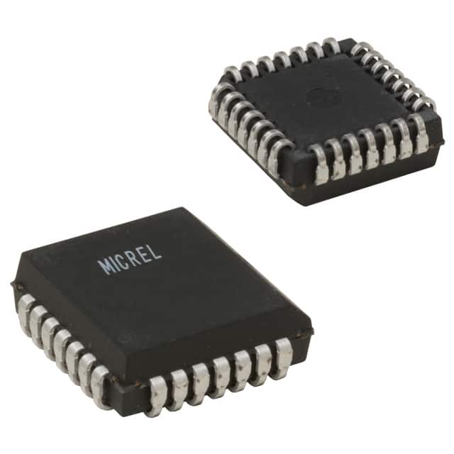
- Package: LJC (Leadless Chip Carrier)
- Essence: Single-ended ECL (Emitter-Coupled Logic) Gate
- Packaging/Quantity: Tape and Reel, 2500 units per reel
Specifications and Parameters
- Supply Voltage: -4.2V to -5.7V
- Input Voltage: -4.2V to -5.7V
- Output Voltage: -4.2V to -5.7V
- Operating Temperature: -40°C to +85°C
- Propagation Delay: 1.3 ns (typical)
- Power Dissipation: 500 mW (max)
Pin Configuration
The SY100E111LJC has a total of 20 pins arranged as follows:
```
| | --| VEE VCC |-- --| GND Qn |-- --| /Qn CLK |-- --| D Dn |-- --| /D R |-- --| S /S |-- --| /R /CLR|-- --| /CLK /CLK |-- --| /GND GND |-- --| /VEE VEE |-- |_______________| ```
Functional Characteristics
The SY100E111LJC is a single-ended ECL gate with the following functional characteristics:
- Differential Clock and Data Inputs
- Asynchronous Reset and Set Inputs
- Complementary Outputs (Q and /Q)
- Clear Input (/CLR) for synchronous reset
- Power-down Mode (/PD) for reduced power consumption
Advantages and Disadvantages
Advantages: - High-speed operation - Low-power consumption - Wide operating temperature range
Disadvantages: - Requires negative supply voltage - Limited availability in certain packages
Applicable Range of Products
The SY100E111LJC is suitable for applications requiring high-speed digital logic gates, such as:
- Data communication systems
- Networking equipment
- Industrial control systems
- Test and measurement instruments
Working Principles
The SY100E111LJC operates based on the principles of Emitter-Coupled Logic (ECL). It uses differential inputs to achieve high-speed operation and provides complementary outputs.
Detailed Application Field Plans
The SY100E111LJC can be used in various applications, including:
- High-speed data transmission systems
- Clock distribution networks
- Digital signal processing circuits
- Frequency synthesizers
- Pulse generation circuits
Detailed Alternative Models
Some alternative models to the SY100E111LJC are:
- SY10EP11LJC
- SY100EL11LJC
- MC10E111FN
5 Common Technical Questions and Answers
Q: What is the maximum operating temperature of the SY100E111LJC? A: The maximum operating temperature is +85°C.
Q: Can I use a positive supply voltage with this IC? A: No, the SY100E111LJC requires a negative supply voltage.
Q: What is the power dissipation of this IC? A: The maximum power dissipation is 500 mW.
Q: Does this IC have a power-down mode? A: Yes, it has a power-down mode (/PD) for reduced power consumption.
Q: What is the typical propagation delay of the SY100E111LJC? A: The typical propagation delay is 1.3 ns.
This encyclopedia entry provides an overview of the SY100E111LJC integrated circuit, including its basic information, specifications, pin configuration, functional characteristics, advantages and disadvantages, applicable range of products, working principles, detailed application field plans, alternative models, and common technical questions and answers.