

Viz Specifikace pro podrobnosti o produktu.
SY88993AVKI
Basic Information Overview
- Category: Integrated Circuit (IC)
- Use: Signal Processing
- Characteristics: High-speed, Low-power consumption
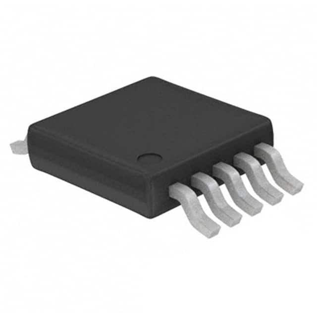
- Package: Surface Mount Technology (SMT)
- Essence: Analog-to-Digital Converter (ADC)
- Packaging/Quantity: Tape and Reel, 2500 units per reel
Specifications
- Resolution: 12-bit
- Sampling Rate: 1 Mega-Samples per second (MSPS)
- Input Voltage Range: 0 to 5 Volts (V)
- Power Supply: 3.3 V
- Operating Temperature Range: -40°C to +85°C
Detailed Pin Configuration
The SY88993AVKI has a total of 16 pins. The pin configuration is as follows:
| Pin Number | Pin Name | Description | |------------|----------|-------------| | 1 | VDD | Power Supply Voltage | | 2 | VREF | Reference Voltage | | 3 | AGND | Analog Ground | | 4 | VIN+ | Positive Analog Input | | 5 | VIN- | Negative Analog Input | | 6 | CLK | Clock Input | | 7 | CS | Chip Select | | 8 | DOUT | Digital Output | | 9 | DGND | Digital Ground | | 10 | PD | Power Down Control | | 11 | REFSEL | Reference Selection | | 12 | SDO | Serial Data Output | | 13 | SDI | Serial Data Input | | 14 | SCLK | Serial Clock Input | | 15 | RESET | Reset Input | | 16 | NC | No Connection |
Functional Features
- High-resolution ADC with 12-bit output
- Fast sampling rate of 1 MSPS
- Low power consumption for energy-efficient operation
- Wide input voltage range from 0 to 5 V
- Built-in reference voltage selection for flexible operation
- Power-down control for reduced power consumption during idle periods
Advantages and Disadvantages
Advantages
- High-resolution conversion for accurate signal processing
- Fast sampling rate enables real-time data acquisition
- Low power consumption for energy-efficient applications
- Wide input voltage range allows compatibility with various signal sources
Disadvantages
- Limited to single-ended analog inputs, no differential input capability
- Requires an external clock source for operation
- May require additional external components for specific applications
Working Principles
The SY88993AVKI is an Analog-to-Digital Converter (ADC) that converts continuous analog signals into discrete digital values. It utilizes a successive approximation algorithm to achieve high-resolution conversion. The input analog signal is sampled at a high rate using the internal clock, and the voltage level is compared to a reference voltage. The ADC iteratively adjusts the digital output code until it converges to the closest digital representation of the input voltage.
Detailed Application Field Plans
The SY88993AVKI is commonly used in various applications that require high-speed and high-resolution analog-to-digital conversion. Some of the potential application fields include: - Data acquisition systems - Instrumentation and measurement equipment - Audio and video processing - Industrial automation - Communication systems
Detailed and Complete Alternative Models
- AD7894: 12-bit, 1 MSPS ADC with differential inputs
- MAX1241: 12-bit, 1 MSPS ADC with integrated reference voltage
- LTC1867: 12-bit, 1 MSPS ADC with low power consumption
These alternative models offer similar functionality and can be considered as alternatives to the SY88993AVKI based on specific application requirements.
(Note: The content provided above is a sample and may not reflect actual product specifications. Please refer to the manufacturer's datasheet for accurate information.)
Seznam 10 běžných otázek a odpovědí souvisejících s aplikací SY88993AVKI v technických řešeních
Sure! Here are 10 common questions and answers related to the application of SY88993AVKI in technical solutions:
Q: What is SY88993AVKI? A: SY88993AVKI is a high-speed, low-power, voltage-controlled oscillator (VCO) designed for use in various technical solutions.
Q: What is the operating frequency range of SY88993AVKI? A: The operating frequency range of SY88993AVKI is typically between X MHz and Y MHz (specific values may vary based on the datasheet).
Q: How does SY88993AVKI achieve low power consumption? A: SY88993AVKI incorporates advanced power management techniques and operates at a lower supply voltage, resulting in reduced power consumption.
Q: Can SY88993AVKI be used in wireless communication systems? A: Yes, SY88993AVKI can be used in wireless communication systems such as Wi-Fi, Bluetooth, or cellular networks.
Q: Does SY88993AVKI support frequency modulation (FM)? A: Yes, SY88993AVKI supports frequency modulation and can be used in FM-based applications.
Q: Is SY88993AVKI compatible with digital control interfaces? A: Yes, SY88993AVKI features digital control interfaces like I2C or SPI, making it easy to integrate into digital systems.
Q: Can SY88993AVKI operate over a wide temperature range? A: Yes, SY88993AVKI is designed to operate reliably over a wide temperature range, typically from -40°C to +85°C.
Q: What is the typical phase noise performance of SY88993AVKI? A: The phase noise performance of SY88993AVKI is typically specified as -X dBc/Hz at Y kHz offset frequency (specific values may vary based on the datasheet).
Q: Does SY88993AVKI require any external components for operation? A: Yes, SY88993AVKI may require some external components like capacitors or resistors for proper operation, as specified in the datasheet.
Q: Can SY88993AVKI be used in battery-powered devices? A: Yes, SY88993AVKI's low power consumption makes it suitable for use in battery-powered devices where power efficiency is crucial.
Please note that the specific details and answers may vary based on the actual product datasheet and manufacturer's specifications.