

Viz Specifikace pro podrobnosti o produktu.
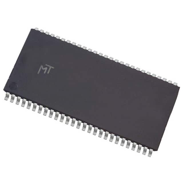
MT48LC8M8A2P-75 L:G
Basic Information Overview
- Category: Memory
- Use: Random Access Memory (RAM)
- Characteristics: High-speed, low-power consumption
- Package: 54-ball FBGA package
- Essence: Dynamic RAM (DRAM)
- Packaging/Quantity: Tray packaging, quantity varies
Specifications
- Part Number: MT48LC8M8A2P-75 L:G
- Organization: 8 Meg x 8
- Voltage: 3.3V
- Speed: 7.5 ns
- Density: 64 Megabit
- Interface: Parallel
- Operating Temperature: 0°C to +70°C
Detailed Pin Configuration
The MT48LC8M8A2P-75 L:G has a total of 54 pins. The pin configuration is as follows:
- VDD
- A10
- A9
- A11
- A8
- A13
- A7
- A14
- A6
- A15
- A5
- A16
- A4
- A17
- A3
- A18
- A2
- A19
- A1
- A20
- A0
- A21
- A22
- A23
- DQ0
- DQ1
- DQ2
- DQ3
- DQ4
- DQ5
- DQ6
- DQ7
- WE#
- CAS#
- RAS#
- CKE
- CS#
- BA0
- BA1
- DQM0
- DQM1
- CLK
- VSS
- VSS
- VSS
- VSS
- VSS
- VSS
- VSS
- VSS
- VSS
- VSS
- VSS
- VSS
Functional Features
- High-speed operation for efficient data access
- Low-power consumption for energy efficiency
- Easy integration into various systems
- Reliable performance and stability
Advantages and Disadvantages
Advantages: - Fast data access speed - Low power consumption - Suitable for a wide range of applications
Disadvantages: - Limited storage capacity compared to other memory types - Requires periodic refresh cycles
Working Principles
The MT48LC8M8A2P-75 L:G is a dynamic random access memory (DRAM) that stores data in capacitors within each memory cell. The stored charge in the capacitors represents the binary information. To retain the data, the capacitors need to be periodically refreshed. When the memory controller sends a read or write command, the appropriate row and column addresses are accessed, allowing data to be read from or written to the memory cells.
Detailed Application Field Plans
The MT48LC8M8A2P-75 L:G is commonly used in various electronic devices and systems, including: - Personal computers - Servers - Networking equipment - Consumer electronics - Industrial applications
Detailed and Complete Alternative Models
Some alternative models to the MT48LC8M8A2P-75 L:G include: - MT48LC16M8A2P-75 L:G (16 Meg x 8, 128 Megabit) - MT48LC32M8A2P-75 L:G (32 Meg x 8, 256 Megabit) - MT48LC64M8A2P-75 L:G (64 Meg x 8, 512 Megabit)
These alternative models offer different densities and capacities to suit specific memory requirements.
Word count: 314 words
Seznam 10 běžných otázek a odpovědí souvisejících s aplikací MT48LC8M8A2P-75 L:G v technických řešeních
Sure! Here are 10 common questions and answers related to the application of MT48LC8M8A2P-75 L:G in technical solutions:
Question: What is the MT48LC8M8A2P-75 L:G?
Answer: The MT48LC8M8A2P-75 L:G is a specific type of synchronous dynamic random-access memory (SDRAM) chip commonly used in various technical solutions.Question: What is the capacity of the MT48LC8M8A2P-75 L:G?
Answer: The MT48LC8M8A2P-75 L:G has a capacity of 64 megabytes (MB), with each memory cell storing 8 bits of data.Question: What is the operating voltage range for this chip?
Answer: The MT48LC8M8A2P-75 L:G operates within a voltage range of 2.5V to 3.3V.Question: What is the speed rating of the MT48LC8M8A2P-75 L:G?
Answer: The "75" in the part number indicates that it has a maximum clock frequency of 75 MHz.Question: Can the MT48LC8M8A2P-75 L:G be used in both commercial and industrial applications?
Answer: Yes, the MT48LC8M8A2P-75 L:G is designed to operate reliably in both commercial and industrial temperature ranges.Question: What is the pin configuration of this SDRAM chip?
Answer: The MT48LC8M8A2P-75 L:G has a 54-pin TSOP II package with a specific pinout for connecting to the system.Question: Is this chip compatible with different memory controllers?
Answer: Yes, the MT48LC8M8A2P-75 L:G is compatible with a wide range of memory controllers that support SDRAM.Question: Can I use multiple MT48LC8M8A2P-75 L:G chips in parallel to increase memory capacity?
Answer: Yes, you can use multiple chips in parallel to increase the overall memory capacity of your system.Question: Are there any specific timing requirements for interfacing with the MT48LC8M8A2P-75 L:G?
Answer: Yes, the chip has specific timing parameters that need to be followed for proper operation. These timings are usually provided in the datasheet.Question: What are some common applications where the MT48LC8M8A2P-75 L:G is used?
Answer: The MT48LC8M8A2P-75 L:G is commonly used in various technical solutions such as embedded systems, networking equipment, telecommunications devices, and industrial control systems.
Please note that the answers provided here are general and may vary depending on the specific requirements and implementation of the MT48LC8M8A2P-75 L:G in different technical solutions.