

Viz Specifikace pro podrobnosti o produktu.
A40MX02-1PLG68I
Product Overview
Category
The A40MX02-1PLG68I belongs to the category of programmable logic devices (PLDs).
Use
This device is primarily used in digital circuit design and implementation. It provides a flexible and customizable solution for various applications.
Characteristics
- Programmable: The A40MX02-1PLG68I can be programmed to perform specific functions based on the user's requirements.
- High Integration: It offers a high level of integration, allowing multiple logic functions to be implemented within a single device.
- Versatile: This PLD supports a wide range of applications due to its programmability.
- Low Power Consumption: The A40MX02-1PLG68I is designed to operate efficiently with low power consumption.
Package
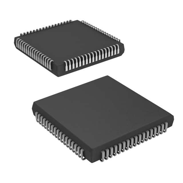
The A40MX02-1PLG68I comes in a PLCC-68 package.
Essence
The essence of this product lies in its ability to provide a reconfigurable logic solution, enabling designers to implement complex digital circuits with ease.
Packaging/Quantity
The A40MX02-1PLG68I is typically packaged individually and is available in various quantities depending on the manufacturer's specifications.
Specifications
- Logic Cells: 2,000
- Maximum Frequency: 100 MHz
- Operating Voltage: 3.3V
- I/O Pins: 68
- Package Type: PLCC-68
Detailed Pin Configuration
The pin configuration of the A40MX02-1PLG68I is as follows:
| Pin Number | Pin Name | Function | |------------|----------|----------| | 1 | VCC | Power Supply (3.3V) | | 2 | GND | Ground | | 3 | IO0 | Input/Output Pin 0 | | 4 | IO1 | Input/Output Pin 1 | | ... | ... | ... | | 68 | IO67 | Input/Output Pin 67 |
Functional Features
- Reconfigurable Logic: The A40MX02-1PLG68I allows users to modify the logic functions according to their specific requirements.
- High-Speed Operation: With a maximum frequency of 100 MHz, this PLD can handle complex digital circuits efficiently.
- I/O Flexibility: The device offers 68 I/O pins, providing flexibility in connecting with external components.
- Low Power Consumption: The A40MX02-1PLG68I is designed to operate with low power consumption, making it suitable for battery-powered applications.
Advantages and Disadvantages
Advantages
- Flexibility: The reconfigurable nature of this PLD allows for easy modifications and updates to the logic design.
- Integration: The high integration level reduces the need for multiple discrete components, saving space and simplifying circuit design.
- Versatility: The A40MX02-1PLG68I supports a wide range of applications due to its programmability.
- Cost-Effective: By eliminating the need for custom-designed ASICs, this PLD offers a cost-effective solution for digital circuit implementation.
Disadvantages
- Learning Curve: Utilizing the full potential of this PLD may require a learning curve for designers who are new to programmable logic devices.
- Limited Resources: The number of logic cells and I/O pins may be insufficient for highly complex designs that require extensive resources.
Working Principles
The A40MX02-1PLG68I operates based on the principles of field-programmable gate arrays (FPGAs). It consists of configurable logic blocks (CLBs), interconnect resources, and I/O elements. The CLBs can be programmed to implement various logic functions, and the interconnect resources allow for the routing of signals between different blocks. The I/O elements provide connectivity with external components.
Detailed Application Field Plans
The A40MX02-1PLG68I finds applications in various fields, including:
- Communications: It can be used in the design of communication systems, such as routers and network switches.
- Industrial Automation: This PLD is suitable for implementing control systems in industrial automation, enabling efficient and flexible operation.
- Consumer Electronics: It can be utilized in consumer electronic devices like gaming consoles, set-top boxes, and multimedia players.
- Automotive: The A40MX02-1PLG68I can be employed in automotive applications, such as engine control units (ECUs) and advanced driver-assistance systems (ADAS).
Detailed and Complete Alternative Models
- A40MX04-1PLG84I: Similar to the A40MX02-1PLG68I, this model offers double the number of logic cells and additional I/O pins.
- A40MX09-1PL
Seznam 10 běžných otázek a odpovědí souvisejících s aplikací A40MX02-1PLG68I v technických řešeních
Sure! Here are 10 common questions and answers related to the application of A40MX02-1PLG68I in technical solutions:
Q1: What is A40MX02-1PLG68I? A1: A40MX02-1PLG68I is a specific model of field-programmable gate array (FPGA) manufactured by Microsemi Corporation.
Q2: What are the key features of A40MX02-1PLG68I? A2: Some key features of A40MX02-1PLG68I include 40,000 usable gates, 2,048 macrocells, 68-pin PLCC package, and support for various I/O standards.
Q3: What are the typical applications of A40MX02-1PLG68I? A3: A40MX02-1PLG68I can be used in various applications such as telecommunications, industrial automation, automotive electronics, medical devices, and more.
Q4: How can A40MX02-1PLG68I be programmed? A4: A40MX02-1PLG68I can be programmed using hardware description languages (HDLs) like VHDL or Verilog, which are then synthesized into a bitstream file that can be loaded onto the FPGA.
Q5: Can A40MX02-1PLG68I be reprogrammed after deployment? A5: Yes, A40MX02-1PLG68I is a reprogrammable FPGA, allowing for flexibility and updates even after it has been deployed in a technical solution.
Q6: What are the power requirements for A40MX02-1PLG68I? A6: The power requirements for A40MX02-1PLG68I typically range from 3.3V to 5V, depending on the specific design and application.
Q7: Does A40MX02-1PLG68I support different I/O standards? A7: Yes, A40MX02-1PLG68I supports various I/O standards such as LVCMOS, LVTTL, LVDS, HSTL, SSTL, and more, making it compatible with a wide range of devices.
Q8: Can A40MX02-1PLG68I interface with other components or devices? A8: Yes, A40MX02-1PLG68I can interface with other components or devices through its I/O pins, allowing for seamless integration into larger systems.
Q9: What are the temperature specifications for A40MX02-1PLG68I? A9: The operating temperature range for A40MX02-1PLG68I is typically between -40°C to +85°C, ensuring reliable performance in various environments.
Q10: Are there any development tools available for working with A40MX02-1PLG68I? A10: Yes, Microsemi provides development tools like Libero SoC Design Suite, which includes synthesis, simulation, and programming tools specifically designed for their FPGAs, including A40MX02-1PLG68I.
Please note that these answers are general and may vary based on specific requirements and documentation provided by the manufacturer.