

Viz Specifikace pro podrobnosti o produktu.
A40MX02-1PQ100
Product Overview
Category
The A40MX02-1PQ100 belongs to the category of programmable logic devices (PLDs).
Use
This device is primarily used for digital circuit design and implementation. It provides a flexible and customizable solution for various applications.
Characteristics
- Programmable: The A40MX02-1PQ100 can be programmed to perform specific functions based on user requirements.
- High Integration: It offers a high level of integration, allowing multiple logic functions to be implemented within a single device.
- Versatile: This PLD supports a wide range of applications due to its programmability.
- Low Power Consumption: The A40MX02-1PQ100 is designed to operate efficiently with low power consumption.
Package
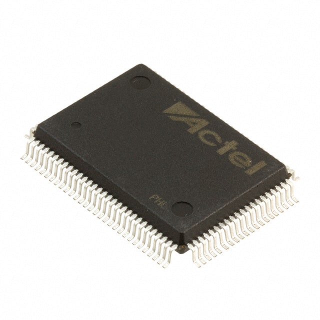
The A40MX02-1PQ100 is available in a PQ100 package. This package type ensures easy installation and compatibility with standard circuit boards.
Essence
The essence of the A40MX02-1PQ100 lies in its ability to provide a reconfigurable hardware platform that enables users to implement complex digital circuits without the need for custom-designed integrated circuits.
Packaging/Quantity
The A40MX02-1PQ100 is typically packaged individually and is available in various quantities depending on the manufacturer's specifications.
Specifications
- Logic Elements: 2,000
- Flip-Flops: 128
- Maximum User I/Os: 96
- Operating Voltage: 3.3V
- Speed Grade: Standard (5ns)
Detailed Pin Configuration
The A40MX02-1PQ100 has a total of 100 pins. The pin configuration is as follows:
- Pin 1: VCCIO
- Pin 2: GND
- Pin 3: IO0
- Pin 4: IO1
- ...
- Pin 99: IO94
- Pin 100: IO95
Functional Features
- Reconfigurability: The A40MX02-1PQ100 can be reprogrammed multiple times, allowing for design changes and updates without the need for hardware modifications.
- High-Speed Operation: This PLD offers fast operation speeds, making it suitable for applications that require real-time processing.
- I/O Flexibility: With a large number of user I/Os, the A40MX02-1PQ100 provides flexibility in connecting to external devices and peripherals.
- Embedded Memory: It includes embedded memory blocks that can be used for data storage or as lookup tables.
Advantages and Disadvantages
Advantages
- Cost-effective: The use of programmable logic devices eliminates the need for custom-designed integrated circuits, reducing development costs.
- Time-saving: The reprogrammability of the A40MX02-1PQ100 allows for faster prototyping and design iterations.
- Versatility: This PLD can be used in various applications, providing a flexible solution for different design requirements.
Disadvantages
- Limited Complexity: Compared to application-specific integrated circuits (ASICs), PLDs have limitations in terms of complexity and performance.
- Power Consumption: While designed for low power consumption, PLDs may still consume more power compared to dedicated integrated circuits.
Working Principles
The A40MX02-1PQ100 utilizes a combination of programmable logic blocks, interconnect resources, and embedded memory to implement digital circuits. The device is programmed using hardware description languages (HDL) or specialized software tools, which generate configuration files that define the desired circuit functionality. These configuration files are then loaded into the PLD, enabling it to perform the specified operations.
Detailed Application Field Plans
The A40MX02-1PQ100 finds applications in various fields, including:
- Communications: It can be used in networking equipment, such as routers and switches, to implement custom protocols and perform packet processing.
- Industrial Automation: The PLD's reconfigurability makes it suitable for controlling and monitoring industrial processes, enabling customization based on specific requirements.
- Automotive Electronics: It can be utilized in automotive systems for functions like engine control, driver assistance, and infotainment systems.
- Consumer Electronics: The A40MX02-1PQ100 can be integrated into consumer electronic devices, such as smart home appliances or multimedia systems, to provide customized features.
Detailed and Complete Alternative Models
A40MX04-1PQ208
- Logic Elements: 4,000
- Flip-Flops: 256
- Maximum User I/Os: 160
- Operating Voltage: 3.3V
- Speed Grade: Standard (5ns)
A40MX09-1PQ160
- Logic Elements: 9,000
- Flip-Flops: 576
- Maximum
Seznam 10 běžných otázek a odpovědí souvisejících s aplikací A40MX02-1PQ100 v technických řešeních
Sure! Here are 10 common questions and answers related to the application of A40MX02-1PQ100 in technical solutions:
1. What is A40MX02-1PQ100? A40MX02-1PQ100 is a specific model of field-programmable gate array (FPGA) manufactured by Microsemi Corporation.
2. What are the key features of A40MX02-1PQ100? Some key features of A40MX02-1PQ100 include 40,000 usable gates, 2,048 macrocells, 64 I/O pins, and a maximum operating frequency of 200 MHz.
3. What are the typical applications of A40MX02-1PQ100? A40MX02-1PQ100 is commonly used in various technical solutions such as digital signal processing, telecommunications, industrial automation, and aerospace applications.
4. How can A40MX02-1PQ100 be programmed? A40MX02-1PQ100 can be programmed using hardware description languages (HDLs) like VHDL or Verilog, which describe the desired functionality of the FPGA.
5. Can A40MX02-1PQ100 be reprogrammed after initial programming? Yes, A40MX02-1PQ100 is a reprogrammable FPGA, allowing for multiple iterations of programming and design changes.
6. What is the power supply requirement for A40MX02-1PQ100? A40MX02-1PQ100 typically requires a single power supply voltage of 3.3V.
7. Does A40MX02-1PQ100 support external memory interfaces? Yes, A40MX02-1PQ100 supports various external memory interfaces such as SDRAM, SRAM, and Flash memory.
8. Can A40MX02-1PQ100 interface with other digital components or microcontrollers? Yes, A40MX02-1PQ100 can interface with other digital components or microcontrollers using standard protocols like SPI, I2C, UART, or GPIO pins.
9. What is the maximum operating temperature range for A40MX02-1PQ100? The maximum operating temperature range for A40MX02-1PQ100 is typically -40°C to +85°C.
10. Are there any development tools available for programming and debugging A40MX02-1PQ100? Yes, Microsemi provides development tools such as Libero SoC Design Suite and SoftConsole IDE for programming, simulation, and debugging of A40MX02-1PQ100-based designs.
Please note that the specific details and answers may vary depending on the manufacturer's documentation and specifications.