

Viz Specifikace pro podrobnosti o produktu.
A54SX08-2VQG100I
Product Overview
Category
A54SX08-2VQG100I belongs to the category of Field Programmable Gate Arrays (FPGAs).
Use
This product is primarily used in digital logic circuits for various applications such as telecommunications, automotive, industrial automation, and consumer electronics.
Characteristics
- High-performance programmable logic device
- Offers flexibility and reconfigurability
- Provides high-speed data processing capabilities
- Supports complex algorithms and computations
- Low power consumption
- Compact size
Package
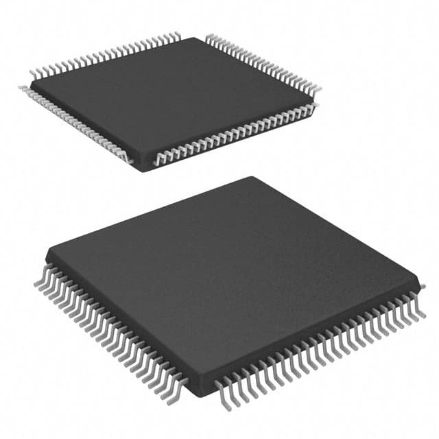
The A54SX08-2VQG100I FPGA is available in a Quad Flat No-Lead (QFN) package.
Essence
The essence of this product lies in its ability to provide a customizable and versatile solution for implementing digital logic circuits.
Packaging/Quantity
The A54SX08-2VQG100I FPGA is typically packaged individually and is available in various quantities depending on the customer's requirements.
Specifications
- Number of Logic Elements: 5,400
- Number of I/O Pins: 100
- Operating Voltage: 1.8V
- Maximum Frequency: 250 MHz
- Embedded Memory: 288 Kbits
- Programmable Interconnects: 3,600
Detailed Pin Configuration
The A54SX08-2VQG100I FPGA has a total of 100 pins, each serving a specific purpose. The pin configuration includes input/output pins, clock pins, power supply pins, and configuration pins. For a detailed pin configuration diagram, please refer to the product datasheet.
Functional Features
- Configurable logic blocks for implementing custom logic functions
- Dedicated arithmetic and DSP blocks for efficient mathematical operations
- On-chip memory for storing data and instructions
- Built-in clock management resources for precise timing control
- Support for various communication protocols such as UART, SPI, and I2C
- Integrated high-speed transceivers for data transmission
Advantages and Disadvantages
Advantages
- Flexibility to modify and reconfigure the logic design as per requirements
- High-performance computing capabilities
- Low power consumption compared to traditional ASICs
- Compact size allows for space-efficient designs
- Cost-effective solution for prototyping and low-volume production
Disadvantages
- Limited scalability compared to Application-Specific Integrated Circuits (ASICs)
- Higher cost per unit compared to mass-produced ASICs
- Requires expertise in FPGA programming and design
Working Principles
The A54SX08-2VQG100I FPGA operates based on the principles of configurable logic. It consists of a matrix of programmable logic elements interconnected through configurable routing resources. The logic elements can be programmed to implement desired digital functions, and the interconnects allow for flexible routing of signals between these elements. The configuration of the FPGA is stored in non-volatile memory and can be modified as needed.
Detailed Application Field Plans
The A54SX08-2VQG100I FPGA finds applications in various fields, including:
- Telecommunications: Used in base stations, network routers, and switches for signal processing and protocol handling.
- Automotive: Employed in automotive electronics for engine control, driver assistance systems, and infotainment systems.
- Industrial Automation: Utilized in programmable logic controllers (PLCs) for process control, monitoring, and automation.
- Consumer Electronics: Integrated into smart TVs, gaming consoles, and home automation systems for enhanced functionality and connectivity.
Detailed and Complete Alternative Models
- A54SX16-2FGG484I: Offers higher logic capacity with 16,000 logic elements.
- A54SX32-2TQG144I: Provides increased I/O pin count and larger embedded memory.
- A54SX64-2FGG484I: Suitable for applications requiring extensive computational capabilities.
These alternative models offer varying specifications to cater to different project requirements.
In conclusion, the A54SX08-2VQG100I FPGA is a high-performance programmable logic device that offers flexibility, reconfigurability, and low power consumption. It finds applications in diverse fields such as telecommunications, automotive, industrial automation, and consumer electronics. With its configurable logic blocks, on-chip memory, and support for various communication protocols, it provides a versatile solution for implementing digital logic circuits. While it has advantages such as flexibility and cost-effectiveness, it also has limitations in terms of scalability and programming expertise required. Nonetheless, the A54SX08-2VQG100I FPGA serves as a valuable tool for designing and prototyping complex digital systems.
Seznam 10 běžných otázek a odpovědí souvisejících s aplikací A54SX08-2VQG100I v technických řešeních
Sure! Here are 10 common questions and answers related to the application of A54SX08-2VQG100I in technical solutions:
Question: What is A54SX08-2VQG100I?
Answer: A54SX08-2VQG100I is a specific model of programmable logic device (PLD) manufactured by Microsemi Corporation.Question: What is the purpose of A54SX08-2VQG100I in technical solutions?
Answer: A54SX08-2VQG100I is used for implementing digital logic functions, such as data processing, control systems, and interface protocols, in various technical applications.Question: What are the key features of A54SX08-2VQG100I?
Answer: Some key features of A54SX08-2VQG100I include 54,000 system gates, 8,192 macrocells, 256 I/O pins, and support for various communication protocols.Question: Can A54SX08-2VQG100I be used in industrial automation applications?
Answer: Yes, A54SX08-2VQG100I is commonly used in industrial automation applications for tasks like process control, monitoring, and data acquisition.Question: Is A54SX08-2VQG100I suitable for high-speed data processing?
Answer: Yes, A54SX08-2VQG100I supports high-speed operation and can handle complex data processing tasks efficiently.Question: Can A54SX08-2VQG100I be programmed using industry-standard design tools?
Answer: Yes, A54SX08-2VQG100I can be programmed using popular design tools like Libero SoC, which provide a user-friendly interface for designing and implementing logic functions.Question: What are the power requirements for A54SX08-2VQG100I?
Answer: A54SX08-2VQG100I typically operates at a voltage range of 3.3V to 5V, depending on the specific application requirements.Question: Can A54SX08-2VQG100I be used in automotive applications?
Answer: Yes, A54SX08-2VQG100I is suitable for automotive applications like engine control units, advanced driver-assistance systems (ADAS), and infotainment systems.Question: Does A54SX08-2VQG100I support secure communication protocols?
Answer: Yes, A54SX08-2VQG100I supports various secure communication protocols like AES encryption, making it suitable for applications that require data security.Question: Are there any limitations or considerations when using A54SX08-2VQG100I?
Answer: Some considerations include understanding the specific requirements of your application, ensuring proper cooling and power management, and verifying compatibility with other components in the system.