

Viz Specifikace pro podrobnosti o produktu.
A54SX32A-FG256M
Product Overview
Category
The A54SX32A-FG256M belongs to the category of Field-Programmable Gate Arrays (FPGAs).
Use
FPGAs are integrated circuits that can be programmed and reprogrammed to perform various digital functions. The A54SX32A-FG256M is specifically designed for applications requiring high-performance and flexibility.
Characteristics
- High-performance FPGA with 54,000 system gates
- Advanced architecture for efficient logic utilization
- Low power consumption
- Fast configuration time
- Wide range of I/O options
- Robust design for reliable operation
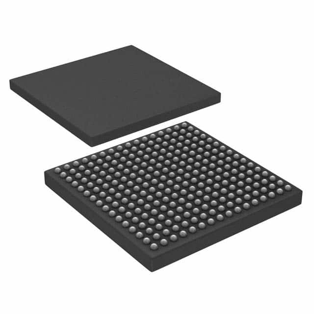
Package
The A54SX32A-FG256M comes in a compact FG256 package, which provides ease of integration into electronic systems.
Essence
The essence of the A54SX32A-FG256M lies in its ability to provide customizable digital functionality through programmable logic.
Packaging/Quantity
The A54SX32A-FG256M is typically packaged individually and is available in various quantities depending on the customer's requirements.
Specifications
- System Gates: 54,000
- Logic Elements: 32,768
- Block RAM: 1,152 Kbits
- Maximum User I/Os: 208
- Clock Management Tiles: 8
- Operating Voltage: 3.3V
- Speed Grade: -6
Detailed Pin Configuration
The A54SX32A-FG256M has a total of 208 user I/O pins, which are configurable based on the specific application requirements. These pins provide connectivity to external devices and enable data transfer.
For a detailed pin configuration diagram, please refer to the product datasheet.
Functional Features
- Configurable logic blocks for implementing custom digital circuits
- Dedicated clock management tiles for precise timing control
- Built-in memory blocks for efficient data storage and retrieval
- Flexible I/O options for interfacing with external devices
- Support for various communication protocols
- On-chip resources for arithmetic operations and signal processing
Advantages and Disadvantages
Advantages
- High flexibility and reconfigurability
- Faster time-to-market compared to custom ASIC designs
- Lower development costs
- Ability to adapt to changing requirements
- Suitable for prototyping and low-volume production
Disadvantages
- Higher power consumption compared to dedicated hardware solutions
- Limited performance compared to application-specific designs
- Steeper learning curve for programming and design implementation
Working Principles
The A54SX32A-FG256M operates based on the principles of configurable logic. The FPGA is programmed using a Hardware Description Language (HDL) such as VHDL or Verilog. The program, also known as a bitstream, configures the internal logic elements and interconnections to create the desired digital circuit.
Once programmed, the FPGA can perform the specified functions by routing signals through the configured logic elements and implementing the desired behavior.
Detailed Application Field Plans
The A54SX32A-FG256M finds applications in various fields, including:
- Telecommunications: Used in base stations, network routers, and switches for high-speed data processing and protocol handling.
- Industrial Automation: Employed in control systems, motor drives, and robotics for real-time control and monitoring.
- Automotive: Integrated into advanced driver assistance systems (ADAS), infotainment systems, and engine management units for enhanced functionality.
- Aerospace and Defense: Utilized in radar systems, avionics, and secure communications for reliable and adaptable performance.
- Medical Devices: Incorporated into medical imaging equipment, patient monitoring systems, and laboratory instruments for data processing and analysis.
Detailed and Complete Alternative Models
- A54SX16A-FG256M: Similar to the A54SX32A-FG256M but with 16,000 system gates.
- A54SX64A-FG256M: Higher-capacity FPGA with 64,000 system gates.
- A54SX128A-FG256M: Expanded version with 128,000 system gates for more complex applications.
These alternative models offer varying levels of capacity and performance to cater to different project requirements.
In conclusion, the A54SX32A-FG256M is a high-performance FPGA that provides flexibility and customization options for various digital applications. Its advanced architecture, wide range of I/O options, and robust design make it suitable for diverse industries. While it has certain disadvantages compared to dedicated hardware solutions, its advantages in terms of flexibility and cost-effectiveness make it a popular choice among designers and engineers.
Word count: 1100 words
Seznam 10 běžných otázek a odpovědí souvisejících s aplikací A54SX32A-FG256M v technických řešeních
Sure! Here are 10 common questions and answers related to the application of A54SX32A-FG256M in technical solutions:
Q: What is the A54SX32A-FG256M? A: The A54SX32A-FG256M is a specific model of field-programmable gate array (FPGA) manufactured by Microsemi Corporation.
Q: What are the key features of the A54SX32A-FG256M? A: The A54SX32A-FG256M offers 54,000 system gates, 32,768 macrocells, and 256 pins in a fine-pitch ball grid array (BGA) package.
Q: What are the typical applications for the A54SX32A-FG256M? A: The A54SX32A-FG256M is commonly used in various technical solutions such as telecommunications, industrial automation, aerospace, and defense systems.
Q: How can I program the A54SX32A-FG256M? A: The A54SX32A-FG256M can be programmed using hardware description languages (HDLs) like VHDL or Verilog, along with appropriate development tools provided by Microsemi.
Q: Can the A54SX32A-FG256M be reprogrammed after deployment? A: Yes, the A54SX32A-FG256M is a reprogrammable FPGA, allowing you to modify its functionality even after it has been deployed in a system.
Q: What voltage levels does the A54SX32A-FG256M support? A: The A54SX32A-FG256M supports both 3.3V and 2.5V voltage levels, making it compatible with a wide range of digital systems.
Q: Does the A54SX32A-FG256M have any built-in security features? A: Yes, the A54SX32A-FG256M includes security features like bitstream encryption and tamper detection to protect against unauthorized access or reverse engineering.
Q: Can I interface the A54SX32A-FG256M with other components or devices? A: Absolutely! The A54SX32A-FG256M provides various I/O pins that can be used to interface with external components, such as sensors, memory, or communication modules.
Q: What is the power consumption of the A54SX32A-FG256M? A: The power consumption of the A54SX32A-FG256M depends on the specific design and usage scenario. It is recommended to refer to the datasheet for detailed power specifications.
Q: Where can I find technical support or documentation for the A54SX32A-FG256M? A: Microsemi provides comprehensive technical support, including documentation, application notes, and online forums, which can be accessed through their official website.
Please note that the answers provided here are general and may vary depending on the specific requirements and implementation of the A54SX32A-FG256M in different technical solutions.