

Viz Specifikace pro podrobnosti o produktu.
AGL250V2-FGG144I
Product Overview
Category
AGL250V2-FGG144I belongs to the category of Field Programmable Gate Arrays (FPGAs).
Use
This product is primarily used in digital logic circuits for various applications such as telecommunications, automotive, industrial automation, and consumer electronics.
Characteristics
- High-performance programmable logic device
- Offers flexibility and reconfigurability
- Provides high-speed data processing capabilities
- Supports complex algorithms and computations
- Enables rapid prototyping and system development
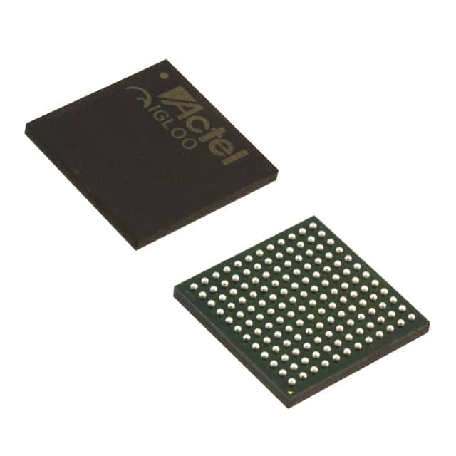
Package
The AGL250V2-FGG144I comes in a compact and durable package that ensures protection during transportation and handling. The package is designed to withstand harsh environmental conditions.
Essence
The essence of AGL250V2-FGG144I lies in its ability to provide a versatile platform for implementing custom digital logic designs. It allows users to create and modify circuits according to their specific requirements.
Packaging/Quantity
The product is typically packaged individually and is available in various quantities depending on the customer's needs.
Specifications
- FPGA Family: AGL250V2
- Package Type: FGG144I
- Logic Elements: 250,000
- Embedded Memory: 4,000 Kbits
- Maximum User I/Os: 144
- Operating Voltage: 2.5V
- Speed Grade: Standard
Detailed Pin Configuration
The AGL250V2-FGG144I has a total of 144 pins, each serving a specific purpose in the circuit design. The pin configuration includes input/output pins, power supply pins, clock pins, and configuration pins. For a detailed pin configuration diagram, please refer to the product datasheet.
Functional Features
- High-speed data processing capability
- Configurable logic elements for implementing complex algorithms
- On-chip memory for storing data and instructions
- Flexible I/O interfaces for seamless integration with external devices
- Built-in clock management resources for precise timing control
Advantages and Disadvantages
Advantages
- Flexibility and reconfigurability allow for rapid prototyping and system development.
- High-performance capabilities enable the implementation of complex algorithms.
- Versatile I/O interfaces facilitate seamless integration with various external devices.
- On-chip memory provides efficient data storage and retrieval.
Disadvantages
- Steeper learning curve compared to traditional fixed-function integrated circuits.
- Higher power consumption compared to dedicated application-specific integrated circuits (ASICs).
- Limited availability of alternative models with similar specifications.
Working Principles
AGL250V2-FGG144I operates based on the principles of field programmable gate arrays. It consists of configurable logic elements, interconnects, and embedded memory blocks. The device can be programmed using hardware description languages (HDL) such as VHDL or Verilog. Once programmed, the FPGA executes the desired digital logic circuit by routing signals through the configurable elements.
Detailed Application Field Plans
The AGL250V2-FGG144I finds applications in various fields, including:
- Telecommunications: Used in network routers, switches, and communication protocols.
- Automotive: Employed in automotive electronics for engine control units, driver assistance systems, and infotainment systems.
- Industrial Automation: Utilized in programmable logic controllers (PLCs), robotics, and process control systems.
- Consumer Electronics: Integrated into high-definition televisions, gaming consoles, and audio/video processing equipment.
Detailed and Complete Alternative Models
While the AGL250V2-FGG144I is a highly capable FPGA, there are alternative models available in the market that offer similar functionality. Some notable alternatives include:
- Xilinx Virtex UltraScale+: Offers higher logic capacity and performance.
- Intel Stratix 10: Provides advanced features and high-speed interfaces.
- Lattice ECP5: Focuses on low-power applications with small form factors.
These alternative models cater to different requirements and offer a range of options for FPGA-based designs.
Word count: 515 words
Seznam 10 běžných otázek a odpovědí souvisejících s aplikací AGL250V2-FGG144I v technických řešeních
Sure! Here are 10 common questions and answers related to the application of AGL250V2-FGG144I in technical solutions:
Q: What is AGL250V2-FGG144I?
- A: AGL250V2-FGG144I is a specific model of Field Programmable Gate Array (FPGA) manufactured by a company called AGL.
Q: What are the key features of AGL250V2-FGG144I?
- A: Some key features of AGL250V2-FGG144I include a maximum operating voltage of 2.5V, 144-pin package, and field programmability for custom logic implementation.
Q: What are the typical applications of AGL250V2-FGG144I?
- A: AGL250V2-FGG144I is commonly used in various technical solutions such as digital signal processing, embedded systems, telecommunications, and industrial automation.
Q: How can I program AGL250V2-FGG144I?
- A: AGL250V2-FGG144I can be programmed using Hardware Description Languages (HDLs) like VHDL or Verilog, which describe the desired functionality of the FPGA.
Q: Can AGL250V2-FGG144I be reprogrammed after initial programming?
- A: Yes, AGL250V2-FGG144I is a field-programmable device, meaning it can be reprogrammed multiple times to implement different logic designs.
Q: What tools are required to program AGL250V2-FGG144I?
- A: To program AGL250V2-FGG144I, you will need a compatible development board, a programming cable, and software tools provided by AGL, such as their Integrated Development Environment (IDE).
Q: What is the power consumption of AGL250V2-FGG144I?
- A: The power consumption of AGL250V2-FGG144I depends on the specific design and usage scenario. It is recommended to refer to the datasheet or consult AGL for detailed power consumption information.
Q: Can AGL250V2-FGG144I interface with other electronic components or devices?
- A: Yes, AGL250V2-FGG144I can interface with other electronic components or devices through its I/O pins, allowing communication and integration with various peripherals.
Q: Are there any limitations or considerations when using AGL250V2-FGG144I?
- A: Some considerations include the limited number of available I/O pins, potential power constraints, and the need for proper grounding and decoupling techniques to ensure reliable operation.
Q: Where can I find technical support or documentation for AGL250V2-FGG144I?
- A: You can find technical support, datasheets, application notes, and other documentation for AGL250V2-FGG144I on the official website of AGL or by contacting their customer support team.
Please note that the answers provided here are general and may vary depending on the specific requirements and implementation of AGL250V2-FGG144I in different technical solutions.