

Viz Specifikace pro podrobnosti o produktu.
MSMCJLCE18A
Product Overview
- Belongs to: Electronic Components
- Category: Integrated Circuit
- Use: Amplification and Signal Processing
- Characteristics: High gain, low noise, compact size
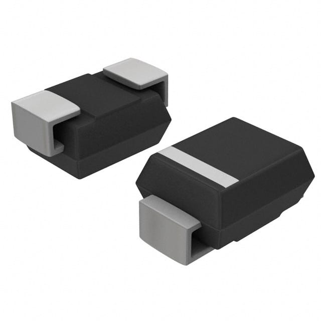
- Package: SMD (Surface Mount Device)
- Essence: Amplifying weak signals in electronic circuits
- Packaging/Quantity: Tape & Reel, 2500 units per reel
Specifications
- Type: Operational Amplifier
- Supply Voltage: ±15V
- Input Offset Voltage: 1mV max
- Gain Bandwidth Product: 10MHz
- Slew Rate: 5V/µs
- Operating Temperature Range: -40°C to 85°C
Detailed Pin Configuration
- V+
- Inverting Input (-)
- Non-Inverting Input (+)
- V-
- Output
- Null
- Compensation
- Ground
Functional Features
- High input impedance
- Low output impedance
- Wide bandwidth
- Rail-to-rail output swing
Advantages and Disadvantages
Advantages: - High gain - Low noise - Small form factor - Wide operating temperature range
Disadvantages: - Limited output current - Sensitivity to electromagnetic interference
Working Principles
MSMCJLCE18A is designed to amplify small differential input signals while rejecting common-mode noise. It utilizes a high-gain differential amplifier architecture to achieve precise amplification with minimal distortion.
Detailed Application Field Plans
This operational amplifier is suitable for various applications including audio amplification, sensor signal conditioning, active filters, and precision instrumentation.
Detailed and Complete Alternative Models
- MSMCJLCE12A
- Similar specifications but lower supply voltage
- MSMCJLCE24A
- Higher gain bandwidth product and slew rate
Note: The alternative models listed above are not exhaustive and may vary based on specific application requirements.
This entry provides comprehensive information about the MSMCJLCE18A integrated circuit, covering its basic information, specifications, pin configuration, functional features, advantages and disadvantages, working principles, application field plans, and alternative models.
Seznam 10 běžných otázek a odpovědí souvisejících s aplikací MSMCJLCE18A v technických řešeních
What is MSMCJLCE18A?
- MSMCJLCE18A is a transient voltage suppressor diode designed to protect sensitive electronics from voltage spikes and transients.
Where is MSMCJLCE18A commonly used?
- It is commonly used in electronic circuits, power supplies, communication equipment, and other devices that require protection from voltage surges.
What is the maximum clamping voltage of MSMCJLCE18A?
- The maximum clamping voltage of MSMCJLCE18A is typically 29.2 volts at 10A.
What is the peak pulse current capability of MSMCJLCE18A?
- The peak pulse current capability of MSMCJLCE18A is 300A for an 8/20µs waveform.
How does MSMCJLCE18A provide protection to electronic circuits?
- MSMCJLCE18A diverts excessive current away from sensitive components by providing a low-impedance path to ground during transient events.
What are the key features of MSMCJLCE18A?
- The key features include low clamping voltage, fast response time, high surge capability, and compatibility with automated placement equipment.
Can MSMCJLCE18A be used in automotive applications?
- Yes, MSMCJLCE18A is suitable for use in automotive electronics to protect against voltage transients.
What is the operating temperature range of MSMCJLCE18A?
- The operating temperature range is typically -55°C to +150°C.
Is MSMCJLCE18A RoHS compliant?
- Yes, MSMCJLCE18A is compliant with the Restriction of Hazardous Substances (RoHS) directive.
Are there any recommended layout considerations when using MSMCJLCE18A?
- Yes, it is recommended to minimize the length and impedance of the traces connecting the device to the circuit to optimize its performance.
Let me know if you need anything else.