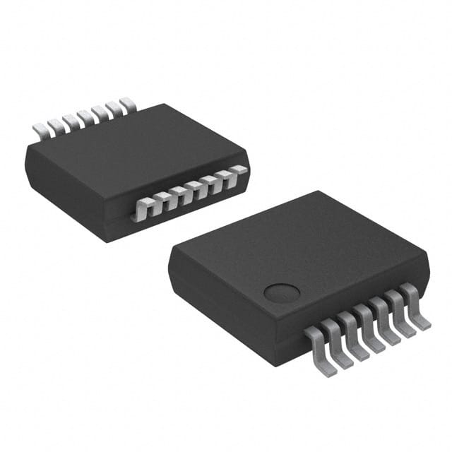
Viz Specifikace pro podrobnosti o produktu.

Encyclopedia Entry: 74ABT125DB,112
Product Overview
- Category: Integrated Circuit (IC)
- Use: Buffer/Line Driver
- Characteristics: High-speed, low-power, non-inverting
- Package: SOIC (Small Outline Integrated Circuit)
- Essence: Logic Level Translator
- Packaging/Quantity: Tape and Reel, 2500 pieces per reel
Specifications
- Supply Voltage Range: 4.5V to 5.5V
- Input Voltage Range: 0V to VCC
- Output Voltage Range: 0V to VCC
- Operating Temperature Range: -40°C to +85°C
- Propagation Delay Time: 3.8ns (typical)
- Output Current: ±24mA
- Input Capacitance: 4pF (typical)
Detailed Pin Configuration
The 74ABT125DB,112 IC has a total of 14 pins, which are numbered as follows:
- OE (Output Enable) - Active Low Output Enable
- 1A (Input) - Input for Channel 1
- 1Y (Output) - Output for Channel 1
- GND (Ground) - Ground Reference
- 2Y (Output) - Output for Channel 2
- 2A (Input) - Input for Channel 2
- 3A (Input) - Input for Channel 3
- 3Y (Output) - Output for Channel 3
- VCC (Supply Voltage) - Positive Power Supply
- 4Y (Output) - Output for Channel 4
- 4A (Input) - Input for Channel 4
- GND (Ground) - Ground Reference
- NC (No Connection) - No Internal Connection
- OE (Output Enable) - Active Low Output Enable
Functional Features
- Non-inverting buffer/line driver with 3-state outputs
- High-speed operation, suitable for high-frequency applications
- Low power consumption, ideal for battery-powered devices
- Provides voltage level translation between different logic families
- 3-state outputs allow multiple devices to share a common bus
Advantages and Disadvantages
Advantages: - High-speed operation enables efficient data transfer - Low power consumption prolongs battery life - 3-state outputs facilitate bus sharing in multi-device systems
Disadvantages: - Limited voltage range (4.5V to 5.5V) - Not suitable for applications requiring higher output current
Working Principles
The 74ABT125DB,112 is a non-inverting buffer/line driver that operates as a voltage level translator. It takes input signals from one logic family and provides compatible output signals for another logic family. The IC uses CMOS technology, which allows for high-speed operation and low power consumption. The 3-state outputs enable the device to be connected to a common bus, allowing multiple devices to share the same communication lines.
Detailed Application Field Plans
The 74ABT125DB,112 IC finds applications in various fields, including: 1. Microcontroller-based systems 2. Data communication networks 3. Industrial automation 4. Automotive electronics 5. Consumer electronics
Detailed and Complete Alternative Models
Some alternative models that can be considered as replacements for the 74ABT125DB,112 IC are: 1. SN74LVC125A - Quad Buffer/Line Driver with 3-State Outputs 2. MC74ACT125 - Quadruple Bus Buffer Gates with 3-State Outputs 3. CD74HCT125E - High-Speed CMOS Logic Quad Buffer with 3-State Outputs
Note: The above alternatives may have different specifications and pin configurations. It is important to refer to their respective datasheets for detailed information.
Word count: 411 words
Seznam 10 běžných otázek a odpovědí souvisejících s aplikací 74ABT125DB,112 v technických řešeních
Sure! Here are 10 common questions and answers related to the application of 74ABT125DB,112 in technical solutions:
Q: What is the function of the 74ABT125DB,112? A: The 74ABT125DB,112 is a quad buffer/line driver with 3-state outputs.
Q: What is the operating voltage range for the 74ABT125DB,112? A: The operating voltage range is typically between 4.5V and 5.5V.
Q: How many buffers/line drivers are there in the 74ABT125DB,112? A: The 74ABT125DB,112 has four buffers/line drivers.
Q: What is the maximum output current of each buffer in the 74ABT125DB,112? A: Each buffer can provide a maximum output current of 24mA.
Q: Can the 74ABT125DB,112 be used for bidirectional communication? A: No, the 74ABT125DB,112 is unidirectional and can only drive signals in one direction.
Q: What is the purpose of the 3-state outputs in the 74ABT125DB,112? A: The 3-state outputs allow the buffers to be disabled, effectively disconnecting them from the output lines.
Q: What is the propagation delay of the 74ABT125DB,112? A: The typical propagation delay is around 4.5ns.
Q: Can the 74ABT125DB,112 handle high-speed signals? A: Yes, the 74ABT125DB,112 is designed for high-speed operation and can handle signals up to several hundred megahertz.
Q: What is the input voltage threshold for the 74ABT125DB,112? A: The input voltage threshold is typically around 2V.
Q: Can the 74ABT125DB,112 be used in automotive applications? A: Yes, the 74ABT125DB,112 is qualified for automotive applications and can operate in harsh environments.
Please note that the answers provided here are general and may vary depending on specific datasheet specifications or application requirements.

