

Viz Specifikace pro podrobnosti o produktu.
74AUP2G79DC,125
Basic Information Overview
- Category: Integrated Circuit (IC)
- Use: Logic Gate
- Characteristics: Dual Positive Edge-Triggered D-Type Flip-Flop
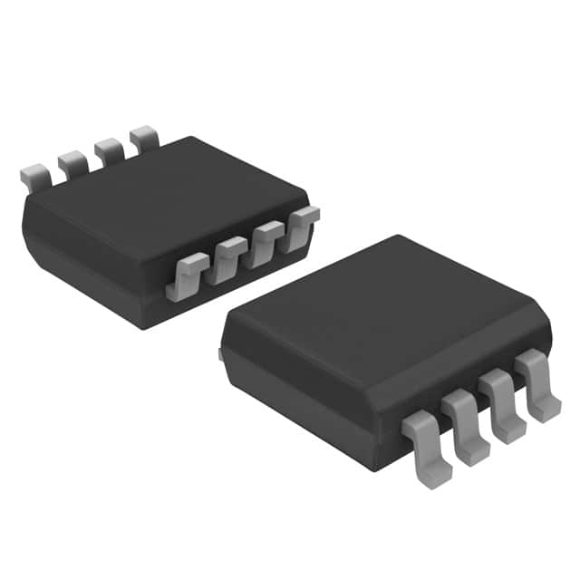
- Package: SOT353 (SC-88A)
- Essence: High-speed CMOS technology
- Packaging/Quantity: Tape and Reel / 3000 pieces per reel
Specifications
- Supply Voltage Range: 0.8V to 3.6V
- High-Level Input Voltage: 0.7 x VCC
- Low-Level Input Voltage: 0.3 x VCC
- High-Level Output Current: -4mA
- Low-Level Output Current: 4mA
- Operating Temperature Range: -40°C to +85°C
Detailed Pin Configuration
The 74AUP2G79DC,125 has a total of 8 pins arranged as follows:
___________
      |           |
   1 -| CLR    VCC |- 8
   2 -| D      Q1  |- 7
   3 -| CP     Q2  |- 6
   4 -| PR     GND |- 5
      |___________|
Functional Features
- Dual positive edge-triggered D-type flip-flop with clear and preset inputs
- High-speed operation due to advanced CMOS technology
- Low power consumption
- Wide supply voltage range allows compatibility with various systems
- Schmitt-trigger action on clock input provides noise immunity
Advantages and Disadvantages
Advantages: - High-speed operation enables efficient data processing - Low power consumption contributes to energy efficiency - Wide supply voltage range enhances compatibility - Noise immunity provided by Schmitt-trigger action ensures reliable operation
Disadvantages: - Limited number of flip-flops in a single package - Sensitive to electrostatic discharge (ESD), requiring proper handling
Working Principles
The 74AUP2G79DC,125 is a dual positive edge-triggered D-type flip-flop. It stores data on the rising edge of the clock signal and provides outputs based on the input data. The clear (CLR) and preset (PR) inputs allow for resetting or setting the flip-flop to specific states. The high-speed operation is achieved through the utilization of advanced CMOS technology.
Detailed Application Field Plans
The 74AUP2G79DC,125 can be used in various applications, including: 1. Digital communication systems 2. Microcontrollers and microprocessors 3. Data storage devices 4. Industrial automation 5. Automotive electronics
Detailed and Complete Alternative Models
Some alternative models that can be considered as replacements for the 74AUP2G79DC,125 are: 1. SN74LVC2G79 - Dual Positive Edge-Triggered D-Type Flip-Flop 2. MC74VHC1G79 - Single Positive Edge-Triggered D-Type Flip-Flop 3. CD4013B - Dual D-Type Flip-Flop
These alternatives offer similar functionality and characteristics, providing flexibility in design choices.
Word count: 238 words
Seznam 10 běžných otázek a odpovědí souvisejících s aplikací 74AUP2G79DC,125 v technických řešeních
Sure! Here are 10 common questions and answers related to the application of 74AUP2G79DC,125 in technical solutions:
Q: What is the function of the 74AUP2G79DC,125? A: The 74AUP2G79DC,125 is a dual positive-edge triggered D-type flip-flop with set and reset inputs.
Q: What is the operating voltage range for the 74AUP2G79DC,125? A: The operating voltage range for this IC is typically between 0.8V and 3.6V.
Q: Can the 74AUP2G79DC,125 be used in battery-powered applications? A: Yes, the low operating voltage range makes it suitable for battery-powered applications.
Q: What is the maximum clock frequency supported by the 74AUP2G79DC,125? A: The maximum clock frequency supported by this IC is typically around 200 MHz.
Q: Does the 74AUP2G79DC,125 have any built-in protection features? A: Yes, it has built-in ESD protection, which helps protect against electrostatic discharge.
Q: Can I use the 74AUP2G79DC,125 in high-speed data transmission applications? A: Yes, this IC can be used in high-speed data transmission applications due to its fast propagation delay.
Q: How many inputs and outputs does the 74AUP2G79DC,125 have? A: It has two data inputs (D1 and D2), two clock inputs (CLK1 and CLK2), and two complementary outputs (Q and Q̅).
Q: Is the 74AUP2G79DC,125 compatible with other logic families? A: Yes, it is compatible with a wide range of logic families, including CMOS and TTL.
Q: Can I cascade multiple 74AUP2G79DC,125 flip-flops together? A: Yes, you can cascade multiple flip-flops to create larger registers or counters.
Q: What are some typical applications for the 74AUP2G79DC,125? A: Some typical applications include data synchronization, frequency division, and general-purpose flip-flop circuits.
Please note that the answers provided here are general and may vary depending on specific datasheet specifications and application requirements.