

Viz Specifikace pro podrobnosti o produktu.
74CBTLVD3384BQ,118
Basic Information Overview
- Category: Integrated Circuit (IC)
- Use: Signal Switching and Routing
- Characteristics: Low Voltage Differential Signaling (LVDS) Interface, High-Speed Operation
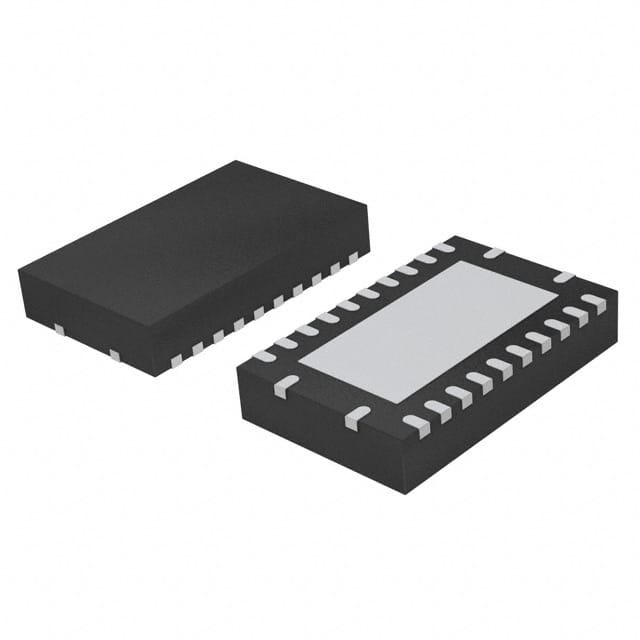
- Package: QFN (Quad Flat No-Lead)
- Essence: Multiplexer/Demultiplexer IC for LVDS Signals
- Packaging/Quantity: Tape and Reel, 3000 pieces per reel
Specifications
- Supply Voltage Range: 1.65V to 3.6V
- Operating Temperature Range: -40°C to +85°C
- Number of Channels: 10
- Data Rate: Up to 2.5 Gbps
- Input Signal Swing: ±100 mV
- On-State Resistance: 4 Ω (typical)
Detailed Pin Configuration
The 74CBTLVD3384BQ,118 IC has a total of 48 pins. The pin configuration is as follows:
| Pin Number | Pin Name | Description | |------------|----------|-------------| | 1 | A0 | Channel Select Input 0 | | 2 | A1 | Channel Select Input 1 | | 3 | A2 | Channel Select Input 2 | | ... | ... | ... | | 46 | Y8 | Output 8 | | 47 | Y9 | Output 9 | | 48 | VCC | Power Supply |
Functional Features
- Low voltage differential signaling (LVDS) interface for high-speed data transmission.
- Wide supply voltage range allows compatibility with various systems.
- 10 channels for multiplexing or demultiplexing LVDS signals.
- Fast switching speed and low on-state resistance ensure minimal signal degradation.
- ESD protection on all pins for enhanced reliability.
Advantages and Disadvantages
Advantages
- High-speed operation enables efficient data transfer.
- LVDS interface provides noise immunity and low power consumption.
- Wide supply voltage range allows flexibility in system integration.
- Compact QFN package offers space-saving benefits.
- ESD protection ensures robustness against electrostatic discharge.
Disadvantages
- Limited number of channels compared to some alternative models.
- May require additional external components for specific applications.
- Higher cost compared to non-LVDS signal switching solutions.
Working Principles
The 74CBTLVD3384BQ,118 is a multiplexer/demultiplexer IC designed for LVDS signals. It operates by selectively routing the input LVDS signals to the desired output channel based on the channel select inputs (A0, A1, A2). The high-speed operation and low on-state resistance ensure minimal signal degradation during switching. The LVDS interface provides noise immunity and low power consumption, making it suitable for high-speed data transmission applications.
Detailed Application Field Plans
The 74CBTLVD3384BQ,118 can be used in various applications that require signal switching and routing with LVDS interface. Some potential application fields include: - Communication systems - Data transmission equipment - Video processing devices - Test and measurement instruments - Industrial automation systems
Detailed and Complete Alternative Models
- SN74CBTLVD3384: Similar LVDS multiplexer/demultiplexer IC from Texas Instruments.
- MC100LVELT23: Differential ECL/LVPECL-to-LVDS translator IC from ON Semiconductor.
- PI3DBS16212: LVDS 16-channel differential switch IC from Diodes Incorporated.
- MAX9126: Quad LVDS line driver/receiver IC from Maxim Integrated.
(Note: This list is not exhaustive and there are other alternative models available in the market.)
This entry provides an overview of the 74CBTLVD3384BQ,118 IC, including its basic information, specifications, pin configuration, functional features, advantages and disadvantages, working principles, application field plans, and alternative models. It serves as a comprehensive reference for users seeking information about this particular LVDS multiplexer/demultiplexer IC.
Seznam 10 běžných otázek a odpovědí souvisejících s aplikací 74CBTLVD3384BQ,118 v technických řešeních
Sure! Here are 10 common questions and answers related to the application of 74CBTLVD3384BQ,118 in technical solutions:
1. What is the purpose of the 74CBTLVD3384BQ,118? The 74CBTLVD3384BQ,118 is a high-bandwidth switch specifically designed for signal switching applications in various technical solutions.
2. What voltage levels does the 74CBTLVD3384BQ,118 support? The 74CBTLVD3384BQ,118 supports voltage levels ranging from 1.65V to 3.6V.
3. How many channels does the 74CBTLVD3384BQ,118 have? The 74CBTLVD3384BQ,118 has 10 channels, allowing for multiple signal paths to be switched.
4. Can the 74CBTLVD3384BQ,118 handle high-speed data signals? Yes, the 74CBTLVD3384BQ,118 is designed to handle high-speed data signals up to 2.5 Gbps.
5. What is the power supply voltage range for the 74CBTLVD3384BQ,118? The power supply voltage range for the 74CBTLVD3384BQ,118 is typically between 1.65V and 3.6V.
6. Does the 74CBTLVD3384BQ,118 support bidirectional signal switching? Yes, the 74CBTLVD3384BQ,118 supports bidirectional signal switching, allowing signals to be routed in both directions.
7. What is the maximum current rating for each channel of the 74CBTLVD3384BQ,118? The maximum current rating for each channel of the 74CBTLVD3384BQ,118 is typically 32 mA.
8. Can the 74CBTLVD3384BQ,118 be used in automotive applications? Yes, the 74CBTLVD3384BQ,118 is AEC-Q100 qualified, making it suitable for use in automotive applications.
9. Does the 74CBTLVD3384BQ,118 have built-in ESD protection? Yes, the 74CBTLVD3384BQ,118 has built-in ESD protection, providing robustness against electrostatic discharge events.
10. What package options are available for the 74CBTLVD3384BQ,118? The 74CBTLVD3384BQ,118 is available in various package options, including TSSOP and HVQFN, to suit different application requirements.
Please note that the answers provided above are general and may vary depending on the specific datasheet and application guidelines provided by the manufacturer.