

Viz Specifikace pro podrobnosti o produktu.
74HC1G126GV,125
Basic Information Overview
- Category: Integrated Circuit (IC)
- Use: Logic Gate Buffer/Driver
- Characteristics: High-speed, low-power, single-gate buffer/driver
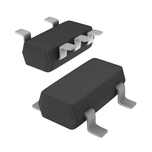
- Package: SOT753 (SC-70-5)
- Essence: Single gate non-inverting buffer/driver
- Packaging/Quantity: Tape and Reel, 3000 pieces per reel
Specifications
- Supply Voltage Range: 2.0V to 6.0V
- Input Voltage Range: GND to VCC
- Output Voltage Range: GND to VCC
- Maximum Operating Frequency: 400 MHz
- Propagation Delay: 4.5 ns (typical)
- Output Current: ±8 mA
- Input Capacitance: 3 pF (typical)
- Power Dissipation: 200 mW
Detailed Pin Configuration
The 74HC1G126GV,125 has a total of 5 pins: 1. Pin 1: Input (A) 2. Pin 2: Enable (E) 3. Pin 3: Ground (GND) 4. Pin 4: Output (Y) 5. Pin 5: Power Supply (VCC)
Functional Features
- Non-inverting buffer/driver with high-speed performance
- Wide supply voltage range allows compatibility with various systems
- Low power consumption makes it suitable for battery-powered devices
- Provides a stable output even with varying input conditions
- Can be used as a level shifter or voltage translator
Advantages and Disadvantages
Advantages: - High-speed operation enables efficient signal processing - Low power consumption prolongs battery life in portable devices - Small package size saves board space - Wide supply voltage range enhances versatility
Disadvantages: - Limited output current may restrict use in certain applications - Input and output voltage ranges are limited to the supply voltage range
Working Principles
The 74HC1G126GV,125 is a single gate non-inverting buffer/driver. It takes an input signal (A) and provides an amplified and buffered output signal (Y). The enable pin (E) controls the operation of the buffer/driver. When the enable pin is high, the buffer/driver is active, and the input signal is passed through to the output. When the enable pin is low, the buffer/driver is disabled, and the output is in a high-impedance state.
Detailed Application Field Plans
The 74HC1G126GV,125 can be used in various applications, including: 1. Signal buffering and level shifting in communication systems 2. Interface translation between different logic families 3. Clock signal distribution in digital circuits 4. Driving capacitive loads in data transmission lines 5. Voltage level conversion in mixed-signal systems
Detailed and Complete Alternative Models
Some alternative models that provide similar functionality to the 74HC1G126GV,125 include: 1. SN74LVC1G126DBVR - Single Gate Buffer/Driver, SOT23-5 package 2. MC74VHC1G126DTT1G - Single Gate Buffer/Driver, SOT353 package 3. TC7SZ126AFK - Single Gate Buffer/Driver, VSSOP-5 package 4. CD74HCT126M96 - Single Gate Buffer/Driver, SOIC-14 package 5. NC7SZ126P5X - Single Gate Buffer/Driver, SC-88A package
These alternative models offer similar features and can be used as substitutes depending on specific requirements and availability.
Word count: 314 words
Seznam 10 běžných otázek a odpovědí souvisejících s aplikací 74HC1G126GV,125 v technických řešeních
Sure! Here are 10 common questions and answers related to the application of 74HC1G126GV,125 in technical solutions:
Q1: What is the 74HC1G126GV,125? A1: The 74HC1G126GV,125 is a single bus buffer gate with 3-state output. It is commonly used in digital logic circuits.
Q2: What is the voltage supply range for the 74HC1G126GV,125? A2: The voltage supply range for the 74HC1G126GV,125 is typically between 2V and 6V.
Q3: What is the maximum output current of the 74HC1G126GV,125? A3: The maximum output current of the 74HC1G126GV,125 is typically around 8mA.
Q4: Can the 74HC1G126GV,125 be used as a level shifter? A4: Yes, the 74HC1G126GV,125 can be used as a level shifter to convert signals between different voltage levels.
Q5: How many inputs does the 74HC1G126GV,125 have? A5: The 74HC1G126GV,125 has one input.
Q6: How many outputs does the 74HC1G126GV,125 have? A6: The 74HC1G126GV,125 has one output.
Q7: Can the 74HC1G126GV,125 drive multiple loads simultaneously? A7: No, the 74HC1G126GV,125 is designed to drive a single load at a time.
Q8: What is the purpose of the 3-state output in the 74HC1G126GV,125? A8: The 3-state output allows the output to be disconnected from the circuit, effectively putting it in a high-impedance state.
Q9: Can the 74HC1G126GV,125 be used in battery-powered applications? A9: Yes, the 74HC1G126GV,125 can be used in battery-powered applications as it operates within a low voltage range.
Q10: What is the typical propagation delay of the 74HC1G126GV,125? A10: The typical propagation delay of the 74HC1G126GV,125 is around 5 nanoseconds.