

Viz Specifikace pro podrobnosti o produktu.
74HC259BQ-Q100,115
Product Overview
- Category: Integrated Circuit (IC)
- Use: Data Storage and Control
- Characteristics: High-Speed, Low-Power, CMOS Logic
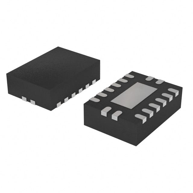
- Package: TSSOP (Thin Shrink Small Outline Package)
- Essence: 8-Bit Addressable Latch/Shift Register
- Packaging/Quantity: Tape and Reel, 2500 units per reel
Specifications
- Supply Voltage Range: 2V to 6V
- Input Voltage Range: 0V to VCC
- Output Voltage Range: 0V to VCC
- Operating Temperature Range: -40°C to +125°C
- Maximum Clock Frequency: 80 MHz
- Maximum Propagation Delay: 20 ns
- Number of Inputs/Outputs: 16
Detailed Pin Configuration
- GND (Ground)
- QA (Output A)
- QB (Output B)
- QC (Output C)
- QD (Output D)
- QE (Output E)
- QF (Output F)
- QG (Output G)
- QH (Output H)
- MR (Master Reset)
- SH/LD (Shift/Load)
- CLK (Clock)
- SER (Serial Data Input)
- A0 (Address Input 0)
- A1 (Address Input 1)
- VCC (Supply Voltage)
Functional Features
- 8-bit parallel-in/serial-out shift register
- Addressable latch functionality
- Serial data input with synchronous clocking
- Master reset for clearing the register
- Shift/load control for selecting between shift and latch modes
Advantages and Disadvantages
Advantages: - High-speed operation - Low power consumption - Wide supply voltage range - Compact TSSOP package - Easy integration into various electronic systems
Disadvantages: - Limited number of inputs/outputs (16) - Not suitable for applications requiring a larger register size
Working Principles
The 74HC259BQ-Q100,115 is an 8-bit addressable latch/shift register. It can store and control data in both parallel and serial formats. The device has eight outputs (QA to QH) that can be individually addressed and controlled. It also features a master reset input (MR) for clearing the register and a shift/load input (SH/LD) for selecting between shift and latch modes.
In shift mode, the register behaves as a serial-in/serial-out shift register. Data is shifted through the register from the serial data input (SER) to the output pins (QA to QH) on each clock pulse. In latch mode, the register acts as an addressable latch, where the state of the inputs (A0 and A1) determines which output pin is latched and holds its value until the next latch operation.
Detailed Application Field Plans
The 74HC259BQ-Q100,115 finds applications in various fields, including:
- Digital Communication Systems: Used for data buffering and multiplexing.
- Industrial Automation: Controls and monitors multiple devices using addressable control signals.
- Automotive Electronics: Provides addressable storage for sensor data and control signals.
- Consumer Electronics: Used in remote control systems, LED displays, and digital audio equipment.
- Computer Peripherals: Enables addressable control of peripheral devices such as printers and scanners.
Detailed and Complete Alternative Models
Some alternative models to the 74HC259BQ-Q100,115 include:
- SN74HC259N by Texas Instruments
- CD74HC259E by Texas Instruments
- MC74HC259AN by ON Semiconductor
- 74HCT259 by NXP Semiconductors
These models offer similar functionality and can be used as alternatives depending on specific requirements.
Word count: 497 words
Seznam 10 běžných otázek a odpovědí souvisejících s aplikací 74HC259BQ-Q100,115 v technických řešeních
Sure! Here are 10 common questions and answers related to the application of 74HC259BQ-Q100,115:
Question: What is the 74HC259BQ-Q100,115?
Answer: The 74HC259BQ-Q100,115 is a high-speed CMOS 8-bit addressable latch with three-state outputs.Question: What is the maximum operating voltage for the 74HC259BQ-Q100,115?
Answer: The maximum operating voltage is 6 volts.Question: How many addressable latches are there in the 74HC259BQ-Q100,115?
Answer: There are 8 addressable latches in the 74HC259BQ-Q100,115.Question: What is the purpose of the three-state outputs in the 74HC259BQ-Q100,115?
Answer: The three-state outputs allow multiple devices to be connected together without bus contention issues.Question: What is the maximum clock frequency for the 74HC259BQ-Q100,115?
Answer: The maximum clock frequency is typically 80 MHz.Question: Can the 74HC259BQ-Q100,115 be used as a shift register?
Answer: No, the 74HC259BQ-Q100,115 is not designed to function as a shift register.Question: What is the power supply range for the 74HC259BQ-Q100,115?
Answer: The power supply range is from 2 volts to 6 volts.Question: Can the 74HC259BQ-Q100,115 be used in automotive applications?
Answer: Yes, the 74HC259BQ-Q100,115 is qualified for automotive applications and meets the AEC-Q100 standard.Question: What is the output current capability of the 74HC259BQ-Q100,115?
Answer: The output current capability is typically 4 mA.Question: Can the 74HC259BQ-Q100,115 be used in both parallel and serial data transfer applications?
Answer: No, the 74HC259BQ-Q100,115 is specifically designed for parallel data transfer applications.
Please note that these answers are general and may vary depending on the specific datasheet and application requirements.