

Viz Specifikace pro podrobnosti o produktu.
74HC373BQ-Q100,115
Basic Information Overview
- Category: Integrated Circuit (IC)
- Use: Octal transparent latch with 3-state outputs
- Characteristics:
- High-speed CMOS technology
- Low power consumption
- Wide operating voltage range
- 3-state outputs for bus-oriented applications
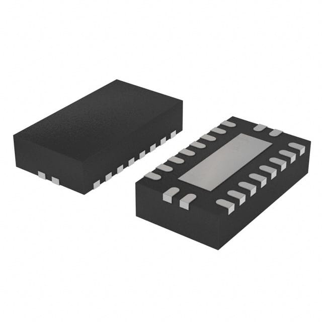
- Package: TSSOP (Thin Shrink Small Outline Package)
- Essence: This IC is designed to provide latch functionality with 3-state outputs, making it suitable for various bus-oriented applications.
- Packaging/Quantity: Available in reels of 2500 pieces
Specifications
- Supply Voltage Range: 2.0V to 6.0V
- Input Voltage Range: 0V to VCC
- Output Voltage Range: 0V to VCC
- Operating Temperature Range: -40°C to +125°C
- Output Current: ±6mA
- Propagation Delay: 11ns (typical)
Detailed Pin Configuration
The 74HC373BQ-Q100,115 IC has a total of 20 pins. The pin configuration is as follows:
- OE (Output Enable) - Output Enable Input
- D0 (Data Input) - Data Input 0
- D1 (Data Input) - Data Input 1
- D2 (Data Input) - Data Input 2
- D3 (Data Input) - Data Input 3
- D4 (Data Input) - Data Input 4
- D5 (Data Input) - Data Input 5
- D6 (Data Input) - Data Input 6
- D7 (Data Input) - Data Input 7
- GND (Ground) - Ground
- Q0 (Output) - Output 0
- Q1 (Output) - Output 1
- Q2 (Output) - Output 2
- Q3 (Output) - Output 3
- Q4 (Output) - Output 4
- Q5 (Output) - Output 5
- Q6 (Output) - Output 6
- Q7 (Output) - Output 7
- LE (Latch Enable) - Latch Enable Input
- VCC (Supply Voltage) - Supply Voltage
Functional Features
- Octal transparent latch with 3-state outputs
- Latch enable input for data storage
- Output enable input for controlling the output state
- High-speed operation suitable for bus-oriented applications
- Low power consumption for energy efficiency
- Wide operating voltage range for versatility
Advantages and Disadvantages
Advantages: - High-speed CMOS technology ensures fast operation - Low power consumption helps in reducing energy usage - 3-state outputs allow for efficient bus-oriented applications - Wide operating voltage range provides flexibility in different systems
Disadvantages: - Limited output current may restrict certain high-power applications - Propagation delay of 11ns may not be suitable for ultra-high-speed operations
Working Principles
The 74HC373BQ-Q100,115 is an octal transparent latch with 3-state outputs. It operates based on the latch enable (LE) and output enable (OE) inputs. When the LE input is high, the data inputs (D0-D7) are latched and stored. The stored data can then be accessed through the corresponding output pins (Q0-Q7). The OE input controls the output state, allowing the outputs to be either active or in a high-impedance state.
Detailed Application Field Plans
The 74HC373BQ-Q100,115 IC finds applications in various fields, including: - Microprocessor systems - Data storage and retrieval systems - Address decoding circuits - Bus-oriented systems - Industrial automation - Communication equipment
Detailed and Complete Alternative Models
Some alternative models that provide similar functionality to the 74HC373BQ-Q100,115 IC are: - SN74HC373N by Texas Instruments - CD74HC373E by Texas Instruments - MC74HC373AN by ON Semiconductor - 74HCT373D by NXP Semiconductors - DM74LS373N by Fairchild Semiconductor
(Note: The above list is not exhaustive and there may be other alternative models available in the market.)
This entry provides a comprehensive overview of the 74HC373BQ-Q100,115 IC, including its basic information, specifications, pin configuration, functional features, advantages and disadvantages, working principles, application field plans, and alternative models.
Seznam 10 běžných otázek a odpovědí souvisejících s aplikací 74HC373BQ-Q100,115 v technických řešeních
Sure! Here are 10 common questions and answers related to the application of 74HC373BQ-Q100,115:
Question: What is the function of the 74HC373BQ-Q100,115?
Answer: The 74HC373BQ-Q100,115 is an octal D-type transparent latch with 3-state outputs.Question: What is the maximum operating voltage for the 74HC373BQ-Q100,115?
Answer: The maximum operating voltage is 6 volts.Question: How many latch outputs does the 74HC373BQ-Q100,115 have?
Answer: It has 8 latch outputs.Question: Can the 74HC373BQ-Q100,115 be used in both parallel and serial data transfer applications?
Answer: Yes, it can be used in both parallel and serial data transfer applications.Question: What is the purpose of the 3-state outputs in the 74HC373BQ-Q100,115?
Answer: The 3-state outputs allow multiple devices to share a common bus without interfering with each other.Question: What is the maximum clock frequency for the 74HC373BQ-Q100,115?
Answer: The maximum clock frequency is typically 25 MHz.Question: Can the 74HC373BQ-Q100,115 be used in high-speed applications?
Answer: Yes, it can be used in high-speed applications due to its fast propagation delay times.Question: Is the 74HC373BQ-Q100,115 compatible with TTL logic levels?
Answer: Yes, it is compatible with TTL logic levels.Question: Does the 74HC373BQ-Q100,115 have any built-in protection features?
Answer: Yes, it has built-in diode clamps to minimize the effects of electrostatic discharge (ESD).Question: Can the 74HC373BQ-Q100,115 be used in automotive applications?
Answer: Yes, it is qualified for automotive applications and meets the AEC-Q100 standard.
Please note that these answers are general and may vary depending on the specific application and requirements. It is always recommended to refer to the datasheet and consult with technical experts for accurate information.