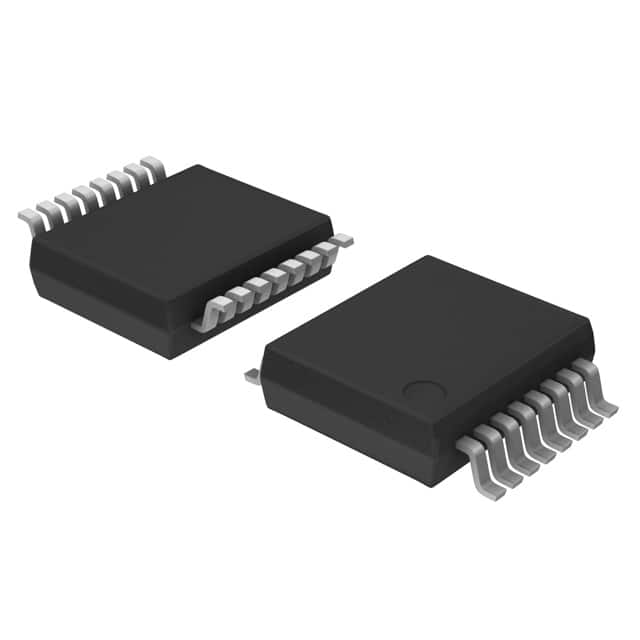
Viz Specifikace pro podrobnosti o produktu.

74HC4050DB,112
Basic Information Overview
- Category: Integrated Circuit (IC)
- Use: Logic Level Shifter
- Characteristics: High-speed CMOS technology, low power consumption
- Package: SOIC (Small Outline Integrated Circuit)
- Essence: Hex Non-Inverting Buffer/Converter
- Packaging/Quantity: Tape and Reel, 2500 pieces per reel
Specifications
- Supply Voltage Range: 2V to 6V
- Input Voltage Range: GND to VCC
- Output Voltage Range: GND to VCC
- Maximum Input Current: ±1mA
- Maximum Output Current: ±25mA
- Propagation Delay: 15ns (typical)
- Operating Temperature Range: -40°C to +125°C
Detailed Pin Configuration
The 74HC4050DB,112 has a total of 16 pins. The pin configuration is as follows:
__    __
   A1 |1  \__/ 16| VCC
   A2 |2        15| Y1
   A3 |3        14| Y2
   A4 |4        13| Y3
   A5 |5   74   12| Y4
   A6 |6 HC4050 11| Y5
  GND |7        10| Y6
   B1 |8         9| Y7
       ----------
Functional Features
- Hex non-inverting buffer with high input impedance
- Converts logic level signals from one voltage level to another
- Provides signal amplification and noise immunity
- Compatible with TTL, CMOS, and MOS logic families
- Wide operating voltage range allows for versatile applications
Advantages and Disadvantages
Advantages: - High-speed operation - Low power consumption - Wide supply voltage range - Compact SOIC package for space-saving designs
Disadvantages: - Limited output current capability - Not suitable for high-power applications
Working Principles
The 74HC4050DB,112 is a hex non-inverting buffer/level shifter. It operates by taking logic level signals from the input pins and converting them to a different voltage level at the corresponding output pins. The device uses high-speed CMOS technology, allowing for fast signal propagation with low power consumption.
Detailed Application Field Plans
The 74HC4050DB,112 can be used in various applications that require logic level shifting or signal buffering. Some common application fields include: - Communication systems - Data transmission - Industrial automation - Consumer electronics - Automotive electronics
Detailed and Complete Alternative Models
- CD4050BE: DIP package, similar functionality
- SN74HC4050N: DIP package, higher operating temperature range
- MC74HC4050ADR2G: SOIC package, wider supply voltage range
These alternative models offer similar functionality to the 74HC4050DB,112 and can be used as replacements depending on specific requirements.
Word count: 314 words
Seznam 10 běžných otázek a odpovědí souvisejících s aplikací 74HC4050DB,112 v technických řešeních
Sure! Here are 10 common questions and answers related to the application of 74HC4050DB,112 in technical solutions:
Q: What is the function of the 74HC4050DB,112? A: The 74HC4050DB,112 is a hex non-inverting buffer with high-to-low level shifting capabilities.
Q: What voltage levels can the 74HC4050DB,112 handle? A: The 74HC4050DB,112 can handle voltages ranging from 2V to 6V.
Q: Can the 74HC4050DB,112 be used for level shifting between different voltage domains? A: Yes, the 74HC4050DB,112 is commonly used for level shifting between different voltage domains.
Q: How many input/output pins does the 74HC4050DB,112 have? A: The 74HC4050DB,112 has six input/output pins.
Q: What is the maximum output current that the 74HC4050DB,112 can provide? A: The 74HC4050DB,112 can provide a maximum output current of 25mA.
Q: Can the 74HC4050DB,112 be used as a logic level converter? A: Yes, the 74HC4050DB,112 can be used as a logic level converter for interfacing between different logic families.
Q: Is the 74HC4050DB,112 compatible with TTL logic levels? A: Yes, the 74HC4050DB,112 is compatible with TTL logic levels.
Q: Can the 74HC4050DB,112 be used for signal amplification? A: No, the 74HC4050DB,112 is not designed for signal amplification. It is primarily used for level shifting and buffering.
Q: What is the power supply voltage range for the 74HC4050DB,112? A: The power supply voltage range for the 74HC4050DB,112 is typically between 2V and 6V.
Q: Can the 74HC4050DB,112 be used in high-speed applications? A: Yes, the 74HC4050DB,112 can be used in high-speed applications as it has a typical propagation delay of 5 ns.
Please note that the answers provided here are general and may vary depending on specific application requirements.

