Viz Specifikace pro podrobnosti o produktu.

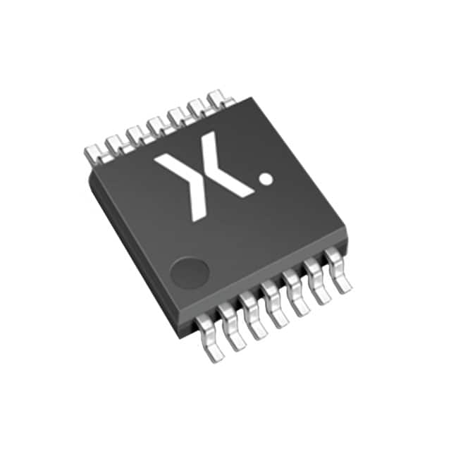
74HC4075PWJ
Product Overview
- Category: Integrated Circuit (IC)
- Use: Logic Gate
- Characteristics: Triple 3-input OR gate
- Package: TSSOP-14
- Essence: High-speed CMOS technology
- Packaging/Quantity: Tape and Reel, 2500 pieces per reel
Specifications
- Supply Voltage Range: 2.0V to 6.0V
- Input Voltage Range: 0V to VCC
- Output Voltage Range: 0V to VCC
- Operating Temperature Range: -40°C to +125°C
- Propagation Delay: 7 ns (typical)
Detailed Pin Configuration
The 74HC4075PWJ has a total of 14 pins, which are assigned as follows:
- Input A1
- Input B1
- Input C1
- Output Y1
- Input A2
- Input B2
- Input C2
- Output Y2
- GND (Ground)
- Input C3
- Input B3
- Input A3
- Output Y3
- VCC (Supply Voltage)
Functional Features
- Triple 3-input OR gate functionality
- High-speed operation due to CMOS technology
- Wide supply voltage range allows for versatile applications
- Low power consumption
- Compatible with TTL and CMOS logic levels
- Schmitt-trigger action on all inputs ensures noise immunity
Advantages and Disadvantages
Advantages: - Versatile and widely used in digital logic circuits - High-speed operation enables efficient data processing - Low power consumption makes it suitable for battery-powered devices - Wide supply voltage range allows for flexibility in various applications - Noise immunity provided by Schmitt-trigger action ensures reliable performance
Disadvantages: - Limited to OR gate functionality, may require additional logic gates for complex operations - Propagation delay of 7 ns may be relatively high for certain applications requiring faster response times
Working Principles
The 74HC4075PWJ is a triple 3-input OR gate that performs logical OR operations on three input signals. It utilizes high-speed CMOS technology, which allows for fast data processing and low power consumption. The Schmitt-trigger action on all inputs ensures noise immunity, making it suitable for applications in noisy environments.
When the input signals are applied, the output Y1, Y2, and Y3 will be driven high if any of the corresponding inputs A1, B1, C1, A2, B2, C2, A3, B3, or C3 are high. Otherwise, the outputs remain low.
Detailed Application Field Plans
The 74HC4075PWJ can be used in various digital logic applications, including but not limited to:
- Data processing systems
- Arithmetic circuits
- Control systems
- Communication devices
- Industrial automation
- Automotive electronics
- Consumer electronics
Its versatility and compatibility with TTL and CMOS logic levels make it a popular choice in these fields.
Detailed and Complete Alternative Models
- CD4075BE: Triple 3-input OR gate, DIP-14 package
- SN74HC4075N: Triple 3-input OR gate, DIP-14 package
- MC74HC4075AN: Triple 3-input OR gate, DIP-14 package
- HCF4075BEY: Triple 3-input OR gate, SOIC-14 package
- TC74HC4075AF: Triple 3-input OR gate, SOP-14 package
These alternative models offer similar functionality and can be used as substitutes for the 74HC4075PWJ in various applications.
Word count: 439 words
Seznam 10 běžných otázek a odpovědí souvisejících s aplikací 74HC4075PWJ v technických řešeních
Sure! Here are 10 common questions and answers related to the application of 74HC4075PWJ in technical solutions:
Q: What is the 74HC4075PWJ? A: The 74HC4075PWJ is a triple 3-input OR gate integrated circuit (IC) that can be used in various digital logic applications.
Q: What is the operating voltage range of the 74HC4075PWJ? A: The 74HC4075PWJ operates within a voltage range of 2V to 6V.
Q: How many OR gates are there in the 74HC4075PWJ? A: The 74HC4075PWJ contains three OR gates, each with three inputs.
Q: Can I use the 74HC4075PWJ for level shifting between different voltage domains? A: No, the 74HC4075PWJ is not designed for level shifting. It is primarily used for logical operations.
Q: What is the maximum output current of the 74HC4075PWJ? A: The maximum output current per gate of the 74HC4075PWJ is typically around 4mA.
Q: Is the 74HC4075PWJ compatible with both TTL and CMOS logic levels? A: Yes, the 74HC4075PWJ is compatible with both TTL and CMOS logic levels, making it versatile for various applications.
Q: Can I connect the outputs of multiple 74HC4075PWJ ICs together? A: Yes, you can connect the outputs of multiple 74HC4075PWJ ICs together to create larger logic functions.
Q: What is the propagation delay of the 74HC4075PWJ? A: The propagation delay of the 74HC4075PWJ is typically around 10ns.
Q: Can I use the 74HC4075PWJ in high-speed applications? A: Yes, the 74HC4075PWJ can be used in high-speed applications due to its relatively low propagation delay.
Q: Are there any specific precautions I should take when using the 74HC4075PWJ? A: It is recommended to follow the datasheet guidelines for proper power supply decoupling and avoid exceeding the maximum ratings specified in the datasheet to ensure reliable operation.
Please note that these answers are general and may vary depending on the specific application and requirements. Always refer to the datasheet and consult with an expert for accurate information.

