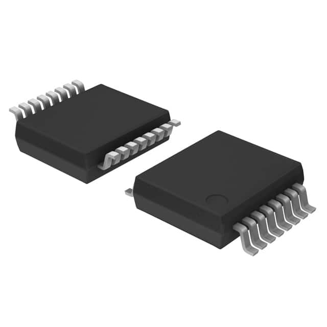
Viz Specifikace pro podrobnosti o produktu.

74HC75DB,118
Product Overview
- Category: Integrated Circuit (IC)
- Use: Digital Logic
- Characteristics: Quad D-type flip-flop; high-speed operation; wide operating voltage range; low power consumption
- Package: SOIC-14
- Essence: Flip-flop circuitry for storing and transferring binary data
- Packaging/Quantity: Tape and Reel, 2500 units per reel
Specifications
- Supply Voltage Range: 2V to 6V
- High-Level Input Voltage: 0.7 x VCC
- Low-Level Input Voltage: 0.3 x VCC
- High-Level Output Voltage: 0.9 x VCC
- Low-Level Output Voltage: 0.1 x VCC
- Maximum Operating Frequency: 80 MHz
- Propagation Delay Time: 18 ns
- Operating Temperature Range: -40°C to +125°C
Detailed Pin Configuration
The 74HC75DB,118 IC has a total of 14 pins arranged as follows:
- Q1: Output of Flip-Flop 1
- D1: Data input for Flip-Flop 1
- CP1: Clock input for Flip-Flop 1
- GND: Ground
- D2: Data input for Flip-Flop 2
- CP2: Clock input for Flip-Flop 2
- Q2: Output of Flip-Flop 2
- Q3: Output of Flip-Flop 3
- D3: Data input for Flip-Flop 3
- CP3: Clock input for Flip-Flop 3
- Q4: Output of Flip-Flop 4
- D4: Data input for Flip-Flop 4
- CP4: Clock input for Flip-Flop 4
- VCC: Supply Voltage
Functional Features
- Quad D-type flip-flop with separate data inputs and clock inputs for each flip-flop
- Non-inverting outputs for Q1, Q2, Q3, and Q4
- High-speed operation allows for efficient data transfer
- Wide operating voltage range enables compatibility with various systems
- Low power consumption for energy-efficient applications
Advantages and Disadvantages
Advantages: - Provides four independent D-type flip-flops in a single package - Compact SOIC-14 package saves board space - High-speed operation allows for quick data processing - Wide operating voltage range ensures versatility - Low power consumption reduces energy usage
Disadvantages: - Limited to digital logic applications - Not suitable for analog signal processing - Requires careful handling due to small package size
Working Principles
The 74HC75DB,118 is based on the principles of D-type flip-flops. Each flip-flop within the IC has a data input (D) and a clock input (CP). When a clock pulse is applied to the CP input, the data at the D input is transferred to the corresponding output (Q). The non-inverting outputs provide the same logic level as the input data.
Detailed Application Field Plans
The 74HC75DB,118 IC finds applications in various digital systems, including but not limited to:
- Data storage and transfer in microcontrollers
- Register circuits in computer architectures
- State machine designs
- Digital communication systems
- Control systems and automation
- Timing and synchronization circuits
Detailed and Complete Alternative Models
Some alternative models that offer similar functionality to the 74HC75DB,118 IC are:
- SN74HC75N by Texas Instruments
- CD4075BE by Texas Instruments
- MC74HC75N by ON Semiconductor
- HEF4075BP by NXP Semiconductors
These alternative models can be considered based on specific requirements and availability.
Word count: 440 words
Seznam 10 běžných otázek a odpovědí souvisejících s aplikací 74HC75DB,118 v technických řešeních
Sure! Here are 10 common questions and answers related to the application of 74HC75DB,118 in technical solutions:
Q: What is the 74HC75DB,118? A: The 74HC75DB,118 is a quad D-type flip-flop IC (integrated circuit) with complementary outputs.
Q: What is the voltage supply range for the 74HC75DB,118? A: The voltage supply range for the 74HC75DB,118 is typically between 2V and 6V.
Q: How many flip-flops are there in the 74HC75DB,118? A: The 74HC75DB,118 contains four independent D-type flip-flops.
Q: What is the maximum clock frequency supported by the 74HC75DB,118? A: The 74HC75DB,118 can operate at a maximum clock frequency of around 25 MHz.
Q: Can the 74HC75DB,118 be used for edge-triggered or level-triggered applications? A: Yes, the 74HC75DB,118 can be used for both edge-triggered and level-triggered applications.
Q: What is the output drive capability of the 74HC75DB,118? A: The 74HC75DB,118 has a typical output drive capability of 5.2 mA.
Q: Is the 74HC75DB,118 compatible with TTL (Transistor-Transistor Logic) inputs? A: Yes, the 74HC75DB,118 is fully compatible with TTL inputs.
Q: Can the 74HC75DB,118 be used in high-speed digital systems? A: Yes, the 74HC75DB,118 is designed for high-speed operation and can be used in various digital systems.
Q: What is the power dissipation of the 74HC75DB,118? A: The power dissipation of the 74HC75DB,118 is typically around 20 mW.
Q: Are there any specific application notes or reference designs available for the 74HC75DB,118? A: Yes, the manufacturer provides application notes and reference designs that can help in implementing the 74HC75DB,118 in different technical solutions.
Please note that these answers are general and may vary depending on the specific datasheet and manufacturer's documentation for the 74HC75DB,118.

