

Viz Specifikace pro podrobnosti o produktu.
74HCT4851BQ-Q100,1
Basic Information Overview
- Category: Integrated Circuit (IC)
- Use: Multiplexer/Demultiplexer
- Characteristics: High-speed CMOS logic, low power consumption
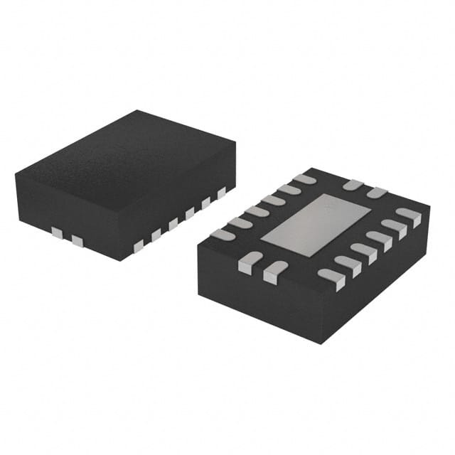
- Package: QFN (Quad Flat No-leads)
- Essence: Analog multiplexer/demultiplexer with digital control
- Packaging/Quantity: Tape and Reel, 2500 units per reel
Specifications
- Supply Voltage Range: 2.0V to 6.0V
- On-state Resistance: 70Ω (typical) at VCC = 4.5V
- Number of Channels: 8 channels
- Input Signal Range: GND to VCC
- Operating Temperature Range: -40°C to +125°C
- Logic Family: HCT
Detailed Pin Configuration
The 74HCT4851BQ-Q100,1 has a total of 16 pins. The pin configuration is as follows:
Pin 1: Channel 0 Select (S0)
Pin 2: Channel 1 Select (S1)
Pin 3: Channel 2 Select (S2)
Pin 4: Channel 3 Select (S3)
Pin 5: Channel 4 Select (S4)
Pin 6: Channel 5 Select (S5)
Pin 7: Channel 6 Select (S6)
Pin 8: Channel 7 Select (S7)
Pin 9: Common Enable (E)
Pin 10: Ground (GND)
Pin 11: Channel 0 Output (Y0)
Pin 12: Channel 1 Output (Y1)
Pin 13: Channel 2 Output (Y2)
Pin 14: Channel 3 Output (Y3)
Pin 15: Channel 4 Output (Y4)
Pin 16: VCC
Functional Features
- Analog multiplexer/demultiplexer with digital control
- Low power consumption
- High-speed CMOS logic
- Wide supply voltage range
- Break-before-make switching action
Advantages and Disadvantages
Advantages: - Versatile multiplexing/demultiplexing capabilities - Low power consumption - High-speed operation - Wide supply voltage range allows compatibility with various systems
Disadvantages: - Limited number of channels (8 channels) - Requires external control signals for channel selection
Working Principles
The 74HCT4851BQ-Q100,1 is an analog multiplexer/demultiplexer that allows the selection of one input signal from multiple sources. It operates based on digital control signals (S0-S7) to select the desired channel. The selected channel's input is then routed to the corresponding output pin (Y0-Y4). The common enable pin (E) is used to enable or disable the device.
Detailed Application Field Plans
The 74HCT4851BQ-Q100,1 finds applications in various fields, including: 1. Audio/Video Switching Systems: Used to route audio/video signals from multiple sources to a single output device. 2. Data Acquisition Systems: Enables the selection of different sensor inputs for data acquisition purposes. 3. Communication Systems: Facilitates the switching of signals between different communication channels. 4. Industrial Control Systems: Allows the selection of different control signals for industrial automation processes.
Detailed and Complete Alternative Models
Some alternative models to the 74HCT4851BQ-Q100,1 include: - CD4051B: 8-channel analog multiplexer/demultiplexer - ADG508A: 8-channel CMOS analog multiplexer - SN74HC151: 8-input multiplexer with 3-state outputs
These alternative models offer similar functionality and can be used as substitutes depending on specific requirements.
Word count: 346 words
Seznam 10 běžných otázek a odpovědí souvisejících s aplikací 74HCT4851BQ-Q100,1 v technických řešeních
Sure! Here are 10 common questions and answers related to the application of 74HCT4851BQ-Q100,1 in technical solutions:
1. What is the function of the 74HCT4851BQ-Q100,1? The 74HCT4851BQ-Q100,1 is a high-speed CMOS analog multiplexer/demultiplexer IC. It allows multiple analog signals to be routed to a single output or vice versa.
2. What is the voltage range supported by the 74HCT4851BQ-Q100,1? The 74HCT4851BQ-Q100,1 supports a wide voltage range from 2V to 10V.
3. How many channels does the 74HCT4851BQ-Q100,1 have? The 74HCT4851BQ-Q100,1 has 8 channels, which means it can handle up to 8 different analog signals.
4. Can the 74HCT4851BQ-Q100,1 be used for both multiplexing and demultiplexing? Yes, the 74HCT4851BQ-Q100,1 can be used for both multiplexing (combining multiple inputs into one output) and demultiplexing (routing one input to multiple outputs).
5. What is the maximum frequency supported by the 74HCT4851BQ-Q100,1? The 74HCT4851BQ-Q100,1 can operate at frequencies up to 125 MHz, making it suitable for high-speed applications.
6. Is the 74HCT4851BQ-Q100,1 compatible with TTL logic levels? Yes, the 74HCT4851BQ-Q100,1 is compatible with both CMOS and TTL logic levels, making it versatile for various applications.
7. Can the 74HCT4851BQ-Q100,1 handle both analog and digital signals? Yes, the 74HCT4851BQ-Q100,1 can handle both analog and digital signals, allowing for mixed-signal applications.
8. What is the power supply voltage range for the 74HCT4851BQ-Q100,1? The 74HCT4851BQ-Q100,1 operates with a power supply voltage range from 2V to 10V.
9. Does the 74HCT4851BQ-Q100,1 have built-in protection features? Yes, the 74HCT4851BQ-Q100,1 has built-in ESD protection, which helps safeguard against electrostatic discharge.
10. Can the 74HCT4851BQ-Q100,1 be cascaded to increase the number of channels? Yes, multiple 74HCT4851BQ-Q100,1 ICs can be cascaded together to increase the number of channels and expand the multiplexing/demultiplexing capabilities.
Please note that these answers are general and may vary depending on the specific application and requirements.