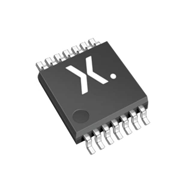
Viz Specifikace pro podrobnosti o produktu.

74LVC125APW,118
Basic Information Overview
- Category: Integrated Circuit (IC)
- Use: Buffer/Line Driver
- Characteristics: Low Voltage CMOS Quad Buffer with 3-State Outputs
- Package: TSSOP-14
- Essence: This IC is designed to provide buffering and line driving capabilities in low voltage applications.
- Packaging/Quantity: The 74LVC125APW,118 is typically sold in reels of 2,500 units.
Specifications
- Supply Voltage Range: 1.65V to 5.5V
- High-Level Input Voltage: 0.7 x VCC
- Low-Level Input Voltage: 0.3 x VCC
- High-Level Output Voltage: 0.9 x VCC
- Low-Level Output Voltage: 0.1 x VCC
- Maximum Operating Frequency: 400 MHz
- Number of Buffers: 4
Detailed Pin Configuration
The 74LVC125APW,118 has a TSSOP-14 package with the following pin configuration:
__    __
   Y1 | 1    14 | VCC
   Y2 | 2    13 | GND
   A1 | 3    12 | B1
   A2 | 4    11 | Y3
   B2 | 5    10 | A3
  GND | 6     9 | B3
   Y4 | 7     8 | A4
       ¯¯    ¯¯
Functional Features
- Quad Buffer: The 74LVC125APW,118 consists of four independent buffer gates that can be used to amplify and drive signals.
- 3-State Outputs: Each buffer gate has a 3-state output, allowing for high impedance when not actively driving a signal.
- Low Voltage Operation: This IC is designed to operate at low voltage levels, making it suitable for use in battery-powered devices.
Advantages and Disadvantages
Advantages: - Low voltage operation allows for compatibility with a wide range of systems. - 3-state outputs provide flexibility in signal routing and control. - Compact TSSOP-14 package saves board space.
Disadvantages: - Limited number of buffer gates (4) may not be sufficient for complex applications requiring more channels. - Maximum operating frequency (400 MHz) may not meet the requirements of high-speed applications.
Working Principles
The 74LVC125APW,118 operates by receiving input signals on the A1-A4 pins. These signals are then amplified and buffered by the internal circuitry. The resulting output signals are available on the Y1-Y4 pins. When the output is not required, the 3-state feature can be used to put the outputs in a high impedance state.
Detailed Application Field Plans
The 74LVC125APW,118 is commonly used in various electronic applications, including but not limited to: - Microcontrollers and microprocessors - Communication systems - Data transmission and reception - Signal level shifting - Bus interfacing
Detailed and Complete Alternative Models
Some alternative models that offer similar functionality to the 74LVC125APW,118 include: - SN74LVC125A: Similar low voltage quad buffer with 3-state outputs from Texas Instruments. - MC74VHC125: Quad buffer with 3-state outputs from ON Semiconductor. - CD74HCT125: Quad buffer with 3-state outputs from Texas Instruments.
These alternative models can be considered based on specific application requirements and availability.
Seznam 10 běžných otázek a odpovědí souvisejících s aplikací 74LVC125APW,118 v technických řešeních
Sure! Here are 10 common questions and answers related to the application of 74LVC125APW,118 in technical solutions:
Q: What is the function of the 74LVC125APW,118? A: The 74LVC125APW,118 is a quad buffer/line driver with 3-state outputs. It is used to amplify and buffer digital signals.
Q: What is the operating voltage range of the 74LVC125APW,118? A: The operating voltage range is typically between 1.65V and 5.5V.
Q: Can the 74LVC125APW,118 be used for level shifting? A: Yes, the 74LVC125APW,118 can be used for level shifting as it supports both 3.3V and 5V logic levels.
Q: How many channels does the 74LVC125APW,118 have? A: The 74LVC125APW,118 has four independent channels.
Q: What is the maximum output current of the 74LVC125APW,118? A: The maximum output current per channel is typically 24mA.
Q: Can the 74LVC125APW,118 drive capacitive loads? A: Yes, the 74LVC125APW,118 can drive capacitive loads up to 50pF.
Q: Is the 74LVC125APW,118 compatible with TTL inputs? A: Yes, the 74LVC125APW,118 is compatible with TTL inputs as it has TTL-compatible input thresholds.
Q: Does the 74LVC125APW,118 have internal pull-up or pull-down resistors? A: No, the 74LVC125APW,118 does not have internal pull-up or pull-down resistors.
Q: What is the propagation delay of the 74LVC125APW,118? A: The typical propagation delay is around 4.3ns.
Q: Can the 74LVC125APW,118 be used in high-speed applications? A: Yes, the 74LVC125APW,118 is suitable for high-speed applications as it has a maximum frequency of 500MHz.
Please note that the answers provided here are general and may vary depending on specific datasheet specifications and application requirements.

