

Viz Specifikace pro podrobnosti o produktu.
74LVC162373ADL,112
Basic Information Overview
- Category: Integrated Circuit (IC)
- Use: Data storage and transfer
- Characteristics: High-speed, low-voltage, 16-bit transparent latch/flip-flop with 3-state outputs
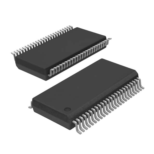
- Package: TSSOP (Thin Shrink Small Outline Package)
- Essence: Latch/flip-flop for digital data storage and transfer
- Packaging/Quantity: Tape and reel packaging, 2500 units per reel
Specifications
- Logic Family: LVC (Low Voltage CMOS)
- Number of Bits: 16
- Output Type: 3-state
- Supply Voltage Range: 1.65V to 5.5V
- Input Voltage Range: 0V to VCC
- Operating Temperature Range: -40°C to +85°C
- Propagation Delay: 4.3 ns (typical)
- Output Current: ±24 mA
- ESD Protection: Human Body Model >2000V
Detailed Pin Configuration
The 74LVC162373ADL,112 IC has a total of 48 pins. The pin configuration is as follows:
+-------------------+
   OE --|1                48|-- VCC
  GND --|2                47|-- A1
   D0 --|3                46|-- B1
   D1 --|4                45|-- C1
   D2 --|5                44|-- D1
   D3 --|6                43|-- E1
   D4 --|7                42|-- F1
   D5 --|8                41|-- G1
   D6 --|9                40|-- H1
   D7 --|10               39|-- I1
   D8 --|11               38|-- J1
   D9 --|12               37|-- K1
  D10 --|13               36|-- L1
  D11 --|14               35|-- M1
  D12 --|15               34|-- N1
  D13 --|16               33|-- O1
  D14 --|17               32|-- P1
  D15 --|18               31|-- Q1
   G1 --|19               30|-- R1
   G2 --|20               29|-- S1
   A1 --|21               28|-- T1
   B1 --|22               27|-- U1
   C1 --|23               26|-- V1
   D1 --|24               25|-- W1
        +-------------------+
Functional Features
- Transparent latch/flip-flop operation for data storage and transfer
- 3-state outputs allow multiple devices to share a common bus
- High-speed operation suitable for applications requiring fast data transfer
- Low-voltage operation makes it compatible with various digital systems
Advantages and Disadvantages
Advantages: - High-speed operation enables efficient data transfer - Low-voltage operation reduces power consumption - 3-state outputs facilitate bus sharing among multiple devices
Disadvantages: - Limited number of bits (16) may not be sufficient for certain applications - Requires careful handling due to sensitivity to electrostatic discharge (ESD)
Working Principles
The 74LVC162373ADL,112 is a latch/flip-flop IC that stores and transfers digital data. It operates on a low voltage supply and features 3-state outputs, allowing multiple devices to share a common bus. The transparent latch/flip-flop functionality ensures that the input data is latched and transferred to the output only when the latch enable (LE) input is high. The output enable (OE) input controls the tri-state outputs, enabling or disabling their connection to the bus.
Detailed Application Field Plans
The 74LVC162373ADL,112 IC finds applications in various fields, including: 1. Data communication systems 2. Computer peripherals 3. Industrial automation 4. Automotive electronics 5. Consumer electronics
Detailed and Complete Alternative Models
Some alternative models that can be considered as alternatives to the 74LVC162373ADL,112 IC are: - SN74LVC162373ADGGR - MC74LVC162373ADG - CD74LVC162373ADGGR - 74LVC162373ADGGRE4
These alternative models offer similar functionality and characteristics, providing options for different sourcing and pricing considerations.
Word count: 411
Seznam 10 běžných otázek a odpovědí souvisejících s aplikací 74LVC162373ADL,112 v technických řešeních
Sure! Here are 10 common questions and answers related to the application of 74LVC162373ADL,112 in technical solutions:
Q: What is the function of the 74LVC162373ADL,112? A: The 74LVC162373ADL,112 is an octal D-type transparent latch with 3-state outputs. It can store and output data based on control signals.
Q: What is the maximum operating voltage for the 74LVC162373ADL,112? A: The maximum operating voltage for the 74LVC162373ADL,112 is typically 3.6V.
Q: How many latch outputs does the 74LVC162373ADL,112 have? A: The 74LVC162373ADL,112 has 8 latch outputs, making it suitable for applications requiring multiple data storage.
Q: Can the 74LVC162373ADL,112 be used in high-speed applications? A: Yes, the 74LVC162373ADL,112 is designed for high-speed operation and can be used in applications that require fast data transfer.
Q: What is the power supply range for the 74LVC162373ADL,112? A: The power supply range for the 74LVC162373ADL,112 is typically between 1.65V and 3.6V.
Q: Does the 74LVC162373ADL,112 support bidirectional data flow? A: Yes, the 74LVC162373ADL,112 supports bidirectional data flow, allowing data to be input and output through the same pins.
Q: Can the 74LVC162373ADL,112 be cascaded to increase the number of latch outputs? A: Yes, multiple 74LVC162373ADL,112 devices can be cascaded together to increase the number of latch outputs in a system.
Q: What is the maximum data transfer rate supported by the 74LVC162373ADL,112? A: The 74LVC162373ADL,112 supports a maximum data transfer rate of typically 400 Mbps.
Q: Is the 74LVC162373ADL,112 compatible with other logic families? A: The 74LVC162373ADL,112 is designed to be compatible with both TTL and CMOS logic families, making it versatile for various applications.
Q: Can the 74LVC162373ADL,112 be used in automotive applications? A: Yes, the 74LVC162373ADL,112 is qualified for automotive applications and meets the necessary standards for reliability and performance in automotive environments.
Please note that the answers provided here are general and may vary depending on specific datasheet specifications and application requirements.