

Viz Specifikace pro podrobnosti o produktu.
Encyclopedia Entry: 74LVC16241ADL,118
Product Overview
Category
The 74LVC16241ADL,118 belongs to the category of integrated circuits (ICs).
Use
This IC is commonly used as a buffer/line driver for various digital applications.
Characteristics
- Low voltage CMOS technology
- High-speed operation
- Wide operating voltage range
- Schmitt-trigger action on all inputs
- Balanced propagation delays
- Symmetrical output impedance
Package
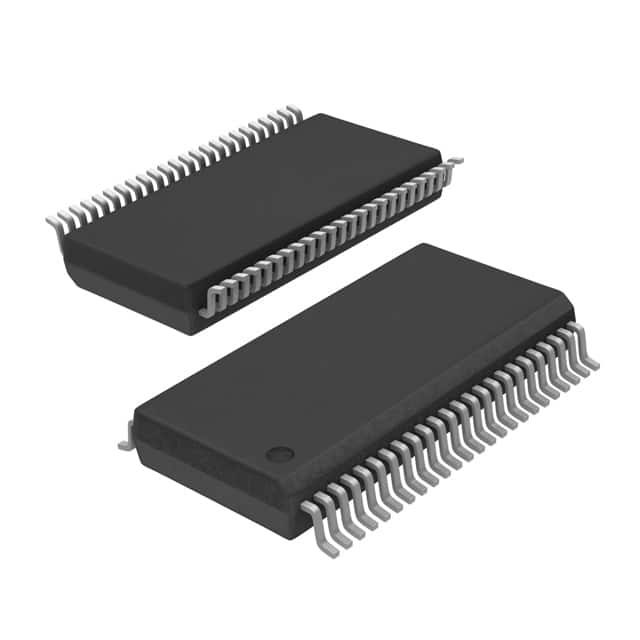
The 74LVC16241ADL,118 is available in a small-outline package (SO) with 48 pins.
Essence
The essence of this product lies in its ability to provide reliable signal buffering and driving capabilities for digital circuits.
Packaging/Quantity
The 74LVC16241ADL,118 is typically packaged in reels or tubes, with a quantity of 2500 units per reel/tube.
Specifications
- Supply voltage: 1.2V to 3.6V
- Input voltage range: 0V to VCC
- Output voltage range: 0V to VCC
- Operating temperature range: -40°C to +85°C
- Maximum input current: ±24mA
- Maximum output current: ±32mA
Detailed Pin Configuration
The 74LVC16241ADL,118 has a total of 48 pins, which are divided into four groups of twelve pins each. The pin configuration is as follows:
Group A: 1. OE1 (Output Enable Input 1) 2. I/O1A (Input/Output 1A) 3. I/O1B (Input/Output 1B) 4. GND (Ground) 5. I/O1C (Input/Output 1C) 6. I/O1D (Input/Output 1D) 7. VCC (Supply Voltage) 8. I/O1E (Input/Output 1E) 9. I/O1F (Input/Output 1F) 10. GND (Ground) 11. I/O1G (Input/Output 1G) 12. I/O1H (Input/Output 1H)
Group B, C, and D have similar pin configurations.
Functional Features
- Buffering: The 74LVC16241ADL,118 provides buffering capabilities to ensure signal integrity and prevent signal degradation.
- Line Driving: It can drive signals over long distances without significant loss or distortion.
- Schmitt-trigger Action: The Schmitt-trigger action on all inputs helps in noise immunity and provides hysteresis for better signal stability.
- Balanced Propagation Delays: The IC ensures balanced propagation delays across all outputs, maintaining synchronization between multiple signals.
Advantages and Disadvantages
Advantages
- Low voltage operation allows compatibility with a wide range of digital systems.
- High-speed operation enables efficient data transfer.
- Schmitt-trigger action enhances noise immunity.
- Symmetrical output impedance simplifies circuit design.
Disadvantages
- Limited output current may restrict its use in certain high-power applications.
- Availability of alternative models with additional features may limit its competitiveness in the market.
Working Principles
The 74LVC16241ADL,118 operates based on CMOS technology. It uses a combination of transistors to amplify and buffer digital signals. When an input signal is received, the IC amplifies it and drives the output with minimal delay and distortion. The Schmitt-trigger action ensures stable output transitions even in the presence of noise.
Detailed Application Field Plans
The 74LVC16241ADL,118 finds applications in various digital systems, including: - Microcontrollers - Data communication systems - Memory interfaces - Industrial automation - Automotive electronics
Detailed and Complete Alternative Models
- 74LVC16244A: Similar to the 74LVC16241ADL,118 but with inverted outputs.
- 74LVCH16245A: Offers higher output current capability for more demanding applications.
- 74LVC16245A: Provides bidirectional level shifting capabilities in addition to buffering.
These alternative models offer similar functionality with slight variations to cater to specific requirements.
In conclusion, the 74LVC16241ADL,118 is a versatile integrated circuit that serves as a buffer/line driver for digital applications. Its low voltage operation, high-speed performance, and Schmitt-trigger action make it suitable for various digital systems. While it has certain limitations, alternative models are available to address specific needs.
Seznam 10 běžných otázek a odpovědí souvisejících s aplikací 74LVC16241ADL,118 v technických řešeních
Sure! Here are 10 common questions and answers related to the application of 74LVC16241ADL,118:
Q: What is the 74LVC16241ADL,118? A: The 74LVC16241ADL,118 is a 16-bit buffer/driver with 3-state outputs. It is designed for low-voltage (2.5V to 3.6V) applications.
Q: What is the purpose of the 74LVC16241ADL,118? A: The purpose of this IC is to provide buffering and driving capabilities for digital signals in various electronic circuits.
Q: What voltage levels does the 74LVC16241ADL,118 support? A: The 74LVC16241ADL,118 supports voltage levels between 2.5V and 3.6V.
Q: How many inputs and outputs does the 74LVC16241ADL,118 have? A: This IC has 16 inputs and 16 outputs.
Q: Can the 74LVC16241ADL,118 be used for bidirectional communication? A: No, the 74LVC16241ADL,118 is a unidirectional buffer/driver and does not support bidirectional communication.
Q: What is the maximum output current of the 74LVC16241ADL,118? A: The maximum output current per channel is typically 32mA.
Q: Can the 74LVC16241ADL,118 handle high-speed signals? A: Yes, this IC is designed for high-speed operation and can handle signals with fast rise and fall times.
Q: Is the 74LVC16241ADL,118 compatible with TTL and CMOS logic levels? A: Yes, this IC is compatible with both TTL and CMOS logic levels.
Q: Can the 74LVC16241ADL,118 be used in automotive applications? A: Yes, the 74LVC16241ADL,118 is qualified for automotive applications and meets the necessary standards.
Q: Are there any specific precautions to consider when using the 74LVC16241ADL,118? A: It is important to follow the recommended operating conditions, such as voltage levels and temperature ranges, specified in the datasheet. Additionally, proper decoupling capacitors should be used to ensure stable operation.