

Viz Specifikace pro podrobnosti o produktu.
74LVC374ABQ-Q100X
Basic Information Overview
- Category: Integrated Circuit (IC)
- Use: Flip-Flop / Latch
- Characteristics: Low-voltage, high-speed, low-power consumption
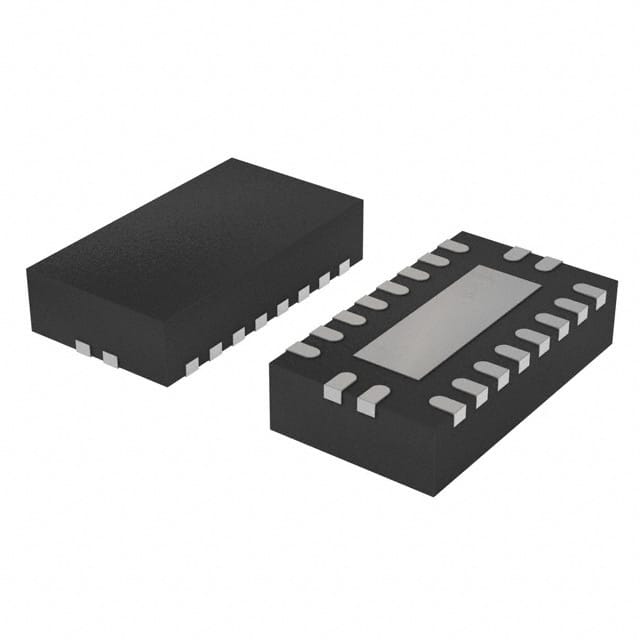
- Package: TSSOP (Thin Shrink Small Outline Package)
- Essence: This IC is a D-type flip-flop with 3-state outputs, designed for low-voltage applications.
- Packaging/Quantity: Available in tape and reel packaging, with a quantity of 2500 units per reel.
Specifications
- Supply Voltage Range: 1.65V to 5.5V
- High-Level Input Voltage: 0.7 x VCC
- Low-Level Input Voltage: 0.3 x VCC
- High-Level Output Voltage: 0.9 x VCC
- Low-Level Output Voltage: 0.1 x VCC
- Maximum Operating Frequency: 200 MHz
- Propagation Delay Time: 4.2 ns (typical)
Detailed Pin Configuration
The 74LVC374ABQ-Q100X IC has a total of 20 pins, which are assigned specific functions. The pin configuration is as follows:
+----+--+----+
   OE --|1   +--+ 20|-- VCC
   D0 --|2         19|-- Q0
   D1 --|3         18|-- Q1
   D2 --|4         17|-- Q2
   D3 --|5         16|-- Q3
   D4 --|6         15|-- Q4
   D5 --|7         14|-- Q5
   D6 --|8         13|-- Q6
   D7 --|9         12|-- Q7
  GND --|10        11|-- CP
        +------------+
Functional Features
- 3-state outputs: The IC provides three-state outputs, allowing multiple devices to share a common bus without interference.
- Edge-triggered flip-flop: The IC operates on the rising edge of the clock signal, capturing the input data and storing it in its internal memory.
- Low-voltage operation: Designed for low-voltage applications, the IC can operate within a wide supply voltage range of 1.65V to 5.5V.
- High-speed operation: With a maximum operating frequency of 200 MHz, the IC enables fast data processing.
- Low-power consumption: The IC is designed to minimize power consumption, making it suitable for battery-powered devices.
Advantages and Disadvantages
Advantages: - Three-state outputs allow for efficient bus sharing. - High-speed operation enables quick data processing. - Low-voltage operation makes it compatible with various systems. - Low-power consumption prolongs battery life in portable devices.
Disadvantages: - Limited number of flip-flops (8 in total). - Not suitable for high-frequency applications.
Working Principles
The 74LVC374ABQ-Q100X is a positive-edge-triggered D-type flip-flop. It stores data at the rising edge of the clock signal (CP). When the clock signal transitions from low to high, the input data (D0-D7) is captured and stored in the flip-flop's internal memory. The stored data is then available at the output pins (Q0-Q7).
Detailed Application Field Plans
The 74LVC374ABQ-Q100X IC finds applications in various fields, including: 1. Microcontrollers: Used for interfacing microcontrollers with external devices, such as sensors and actuators. 2. Communication Systems: Enables data buffering and synchronization in communication systems. 3. Memory Systems: Used in memory address decoding and data storage applications. 4. Industrial Automation: Facilitates control signal generation and synchronization in industrial automation systems.
Detailed and Complete Alternative Models
- 74HC374: Similar functionality, but operates at a higher voltage range (2V to 6V).
- SN74LS374: Compatible with TTL logic levels, but operates at a slower speed compared to the 74LVC374ABQ-Q100X.
- CD4013B: Dual D-type flip-flop IC, suitable for various applications requiring flip-flops.
(Note: The above alternative models are just a few examples and not an exhaustive list.)
This concludes the encyclopedia entry for the 74LVC374ABQ-Q100X IC.
Seznam 10 běžných otázek a odpovědí souvisejících s aplikací 74LVC374ABQ-Q100X v technických řešeních
Sure! Here are 10 common questions and answers related to the application of 74LVC374ABQ-Q100X in technical solutions:
Question: What is the function of the 74LVC374ABQ-Q100X?
Answer: The 74LVC374ABQ-Q100X is an octal D-type flip-flop with 3-state outputs, used for storing and transferring data in digital circuits.Question: What is the operating voltage range of the 74LVC374ABQ-Q100X?
Answer: The operating voltage range is from 1.65V to 5.5V.Question: How many flip-flops are there in the 74LVC374ABQ-Q100X?
Answer: The 74LVC374ABQ-Q100X has 8 flip-flops, making it an octal flip-flop.Question: What is the maximum clock frequency supported by the 74LVC374ABQ-Q100X?
Answer: The maximum clock frequency is typically 125 MHz.Question: Can the 74LVC374ABQ-Q100X be used in both parallel and serial data transfer applications?
Answer: Yes, the 74LVC374ABQ-Q100X can be used for both parallel and serial data transfer, depending on the configuration.Question: Does the 74LVC374ABQ-Q100X have 3-state outputs?
Answer: Yes, the 74LVC374ABQ-Q100X has 3-state outputs, which means they can be in high-impedance state when not actively driving a signal.Question: What is the typical propagation delay of the 74LVC374ABQ-Q100X?
Answer: The typical propagation delay is around 4.5 ns.Question: Can the 74LVC374ABQ-Q100X be used in automotive applications?
Answer: Yes, the 74LVC374ABQ-Q100X is qualified for automotive applications and meets the AEC-Q100 standard.Question: What is the package type of the 74LVC374ABQ-Q100X?
Answer: The 74LVC374ABQ-Q100X comes in a small outline package (SO) with 20 pins.Question: Is the 74LVC374ABQ-Q100X compatible with other logic families?
Answer: Yes, the 74LVC374ABQ-Q100X is compatible with both 3.3V and 5V logic families, making it versatile for various applications.
Please note that these answers are general and may vary depending on the specific datasheet and manufacturer's specifications.