

Viz Specifikace pro podrobnosti o produktu.
74LVC8T595BQX
Basic Information Overview
- Category: Integrated Circuit (IC)
- Use: Shift Register
- Characteristics: Low-voltage, high-speed, and low-power consumption
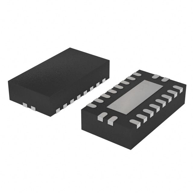
- Package: TSSOP (Thin Shrink Small Outline Package)
- Essence: Serial-in, parallel-out shift register with output latches
- Packaging/Quantity: Tape and Reel, 2500 units per reel
Specifications
- Supply Voltage Range: 1.65V to 5.5V
- High-Level Input Voltage: 0.7 x VCC
- Low-Level Input Voltage: 0.3 x VCC
- High-Level Output Voltage: 0.9 x VCC
- Low-Level Output Voltage: 0.1 x VCC
- Maximum Clock Frequency: 100 MHz
- Operating Temperature Range: -40°C to +125°C
Detailed Pin Configuration
The 74LVC8T595BQX has a total of 20 pins. The pin configuration is as follows:
- SER (Serial Data Input)
- OE (Output Enable)
- RCLK (Register Clock)
- SRCLK (Shift Register Clock)
- SRCLR (Shift Register Clear)
- GND (Ground)
- QA (Parallel Output A)
- QB (Parallel Output B)
- QC (Parallel Output C)
- QD (Parallel Output D)
- QE (Parallel Output E)
- QF (Parallel Output F)
- QG (Parallel Output G)
- QH (Parallel Output H)
- VCC (Supply Voltage)
- DS (Serial Data Output)
- SHCP (Shift Register Clock for Parallel Load)
- STCP (Storage Register Clock)
- MR (Master Reset)
- VCC (Supply Voltage)
Functional Features
- Serial-in, parallel-out shift register with output latches
- 8-bit data storage and transfer capability
- High-speed operation with low power consumption
- Output enable control for easy cascading of multiple devices
- Shift register clear function for initialization
- Parallel load capability for direct data input
Advantages and Disadvantages
Advantages: - Low-voltage operation allows compatibility with a wide range of systems - High-speed performance enables efficient data transfer - Low-power consumption reduces energy requirements - Output enable control simplifies device cascading - Compact TSSOP package offers space-saving benefits
Disadvantages: - Limited number of parallel outputs (8 bits) - Requires external clock signals for proper operation - Sensitivity to voltage fluctuations may affect performance
Working Principles
The 74LVC8T595BQX is a serial-in, parallel-out shift register with output latches. It receives data serially through the SER pin and shifts it into the shift register on each rising edge of the SRCLK signal. The data can be loaded in parallel into the storage register by activating the SHCP pin. The output data can be latched and held using the STCP pin.
Detailed Application Field Plans
The 74LVC8T595BQX is commonly used in various applications, including but not limited to: 1. LED matrix displays 2. LED driver circuits 3. Serial-to-parallel data conversion 4. Data storage and transfer systems 5. Control and automation systems
Detailed and Complete Alternative Models
Some alternative models that offer similar functionality to the 74LVC8T595BQX include: 1. SN74HC595 - High-Speed CMOS Logic Shift Register 2. CD4094 - 8-Stage Shift-and-Store Bus Register 3. 74HC595 - 8-Bit Serial-In, Serial or Parallel-Out Shift Register 4. CD74HC595 - High-Speed CMOS Logic Shift Register
These alternative models can be considered based on specific requirements and compatibility with the target system.
Word Count: 438 words
Seznam 10 běžných otázek a odpovědí souvisejících s aplikací 74LVC8T595BQX v technických řešeních
Sure! Here are 10 common questions and answers related to the application of 74LVC8T595BQX in technical solutions:
Question: What is the purpose of the 74LVC8T595BQX?
Answer: The 74LVC8T595BQX is an 8-bit shift register with output latches, used for serial-to-parallel data conversion.Question: What is the maximum operating voltage for the 74LVC8T595BQX?
Answer: The maximum operating voltage is 5.5V.Question: Can the 74LVC8T595BQX be used with both CMOS and TTL logic levels?
Answer: Yes, it is compatible with both CMOS and TTL logic levels.Question: How many outputs does the 74LVC8T595BQX have?
Answer: It has 8 outputs that can be individually controlled.Question: What is the maximum output current for each output pin?
Answer: The maximum output current per pin is 32mA.Question: Can the 74LVC8T595BQX be cascaded to increase the number of outputs?
Answer: Yes, multiple 74LVC8T595BQX chips can be cascaded to increase the number of outputs.Question: What is the typical clock frequency range for the 74LVC8T595BQX?
Answer: The typical clock frequency range is between 0Hz and 100MHz.Question: Does the 74LVC8T595BQX have any built-in protection features?
Answer: Yes, it has built-in ESD protection up to 2kV.Question: Can the 74LVC8T595BQX be used in both parallel and serial data transfer modes?
Answer: Yes, it can be used in both parallel and serial data transfer modes.Question: What is the power supply voltage range for the 74LVC8T595BQX?
Answer: The power supply voltage range is between 1.65V and 5.5V.
Please note that these answers are general and may vary depending on the specific application and requirements.