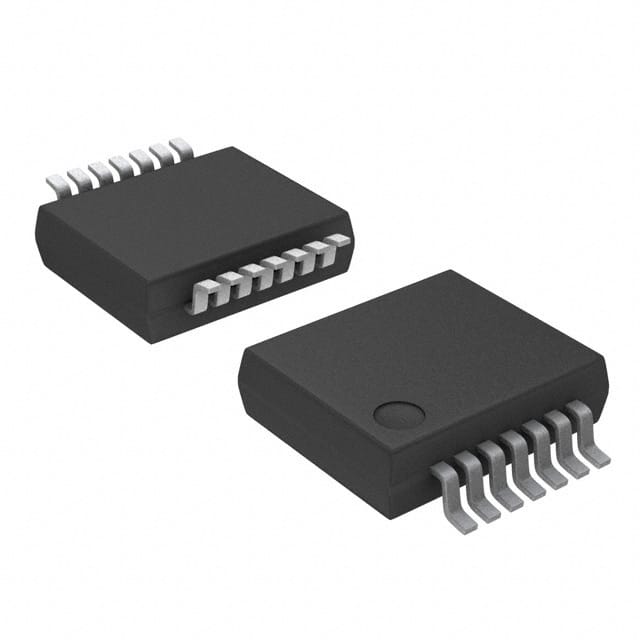
Viz Specifikace pro podrobnosti o produktu.

74LVTH125DB,118
Basic Information Overview
- Category: Integrated Circuit (IC)
- Use: Logic Level Translator
- Characteristics: High-speed, low-power, voltage-level shifting
- Package: SSOP-14
- Essence: Translates signals between different voltage levels
- Packaging/Quantity: Tape and Reel, 2500 units per reel
Specifications
- Supply Voltage Range: 1.65V to 5.5V
- Input Voltage Range: 0V to VCC
- Output Voltage Range: 0V to VCC
- High-Level Input Voltage: 0.7 x VCC to VCC
- Low-Level Input Voltage: 0V to 0.3 x VCC
- High-Level Output Voltage: 0.9 x VCC to VCC
- Low-Level Output Voltage: 0V to 0.1 x VCC
- Maximum Operating Frequency: 400 MHz
Detailed Pin Configuration
The 74LVTH125DB,118 IC has a total of 14 pins arranged as follows:
___________
   OE | 1       14 | VCC
  A1  | 2       13 | B1
  Y1  | 3       12 | A2
  GND | 4       11 | B2
  Y2  | 5       10 | OE#
  A3  | 6        9 | B3
  B3  | 7        8 | Y3
       ‾‾‾‾‾‾‾‾‾‾‾‾
Functional Features
- Bidirectional voltage-level translation
- Supports both 3.3V and 5V systems
- High-speed operation with minimal propagation delay
- Low power consumption
- 3-state outputs for bus-oriented applications
Advantages and Disadvantages
Advantages: - Wide supply voltage range allows compatibility with various systems - High-speed operation enables efficient signal translation - Low power consumption helps in reducing overall system energy usage - 3-state outputs facilitate bus sharing and multiplexing
Disadvantages: - Limited maximum operating frequency compared to some other ICs - SSOP package may require careful handling during assembly
Working Principles
The 74LVTH125DB,118 is a logic level translator that operates by shifting the voltage levels of input signals to match the desired output voltage levels. It utilizes a combination of MOSFETs and CMOS technology to achieve bidirectional voltage translation. The OE (Output Enable) pin controls the direction of translation, allowing the IC to function as a buffer or a level shifter.
Detailed Application Field Plans
The 74LVTH125DB,118 is commonly used in various applications where voltage-level translation is required. Some typical application fields include: - Interfacing between different logic families (e.g., 3.3V and 5V) - Communication systems involving mixed voltage domains - Bus-oriented systems requiring bidirectional signal translation - Microcontroller and FPGA interfacing
Detailed and Complete Alternative Models
- SN74LVC1T45DBVR
- TXB0108PWR
- PCA9306DCUR
- 74LVC245APW,118
- CD4050BE
These alternative models offer similar functionality and can be considered as replacements for the 74LVTH125DB,118 depending on specific requirements and availability.
Word count: 311 words
Seznam 10 běžných otázek a odpovědí souvisejících s aplikací 74LVTH125DB,118 v technických řešeních
Sure! Here are 10 common questions and answers related to the application of 74LVTH125DB,118 in technical solutions:
Q: What is the function of the 74LVTH125DB,118? A: The 74LVTH125DB,118 is a quad buffer/line driver with 3-state outputs. It can be used to amplify and buffer digital signals.
Q: What is the operating voltage range of the 74LVTH125DB,118? A: The 74LVTH125DB,118 operates within a voltage range of 1.65V to 5.5V.
Q: Can the 74LVTH125DB,118 handle high-speed data transmission? A: Yes, the 74LVTH125DB,118 is designed for high-speed operation and can handle data rates up to 400 Mbps.
Q: How many buffers/line drivers are there in the 74LVTH125DB,118? A: The 74LVTH125DB,118 contains four individual buffers/line drivers.
Q: What is the output current capability of the 74LVTH125DB,118? A: The 74LVTH125DB,118 has a typical output current capability of ±32 mA.
Q: Can the 74LVTH125DB,118 be used in bidirectional applications? A: No, the 74LVTH125DB,118 is unidirectional and can only be used for buffering or driving signals in one direction.
Q: Does the 74LVTH125DB,118 have internal pull-up or pull-down resistors? A: No, the 74LVTH125DB,118 does not have internal pull-up or pull-down resistors. External resistors may be required for pull-up or pull-down functionality.
Q: What is the power supply current consumption of the 74LVTH125DB,118? A: The power supply current consumption of the 74LVTH125DB,118 depends on the operating conditions and load, but it typically ranges from 2 mA to 20 mA.
Q: Can the 74LVTH125DB,118 tolerate overvoltage on its inputs? A: Yes, the 74LVTH125DB,118 has input protection that allows it to tolerate voltages up to 7V.
Q: Is the 74LVTH125DB,118 compatible with other logic families? A: Yes, the 74LVTH125DB,118 is designed to be compatible with both TTL and CMOS logic families, making it versatile in various applications.
Please note that these answers are general and may vary depending on specific datasheet specifications and application requirements.

