

Viz Specifikace pro podrobnosti o produktu.
PDTC114YT,215
Product Overview
- Belongs to: Semiconductor category
- Use: Signal switching and amplification in electronic circuits
- Characteristics: Small form factor, high gain, low power consumption
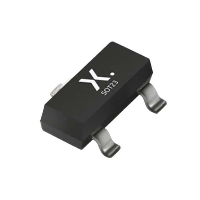
- Package: SOT416 (SC-75)
- Essence: NPN bipolar junction transistor
- Packaging/Quantity: Tape and reel, 3000 units per reel
Specifications
- Collector-Base Voltage (VCBO): 50V
- Collector-Emitter Voltage (VCEO): 45V
- Emitter-Base Voltage (VEBO): 5V
- Collector Current (IC): 100mA
- Power Dissipation (Ptot): 200mW
- Transition Frequency (fT): 250MHz
- Noise Figure (NF): 4dB
Detailed Pin Configuration
- Collector (C)
- Base (B)
- Emitter (E)
Functional Features
- High current gain
- Low noise figure
- Fast switching speed
Advantages
- Small package size
- Suitable for high-frequency applications
- Low power consumption
Disadvantages
- Limited collector current capability
- Susceptible to thermal runaway at high currents
Working Principles
The PDTC114YT,215 operates as a signal amplifier or switch by controlling the flow of current between its collector and emitter terminals based on the input signal applied to its base terminal.
Detailed Application Field Plans
- Audio amplification circuits
- Radio frequency (RF) signal amplification
- Switching circuits in communication systems
Detailed and Complete Alternative Models
- BC847B,235
- MMBT3904LT1G
- 2N3904
This comprehensive entry provides an in-depth understanding of the PDTC114YT,215 semiconductor, covering its specifications, features, advantages, disadvantages, working principles, application field plans, and alternative models.
Seznam 10 běžných otázek a odpovědí souvisejících s aplikací PDTC114YT,215 v technických řešeních
What is the PDTC114YT,215 used for?
- The PDTC114YT,215 is commonly used as a general-purpose NPN transistor in various technical solutions.
What are the key specifications of the PDTC114YT,215?
- The PDTC114YT,215 has a maximum collector current of 100mA, a maximum collector-emitter voltage of 50V, and a DC current gain (hFE) of 100 to 400.
Can the PDTC114YT,215 be used for switching applications?
- Yes, the PDTC114YT,215 can be used for low-power switching applications due to its moderate current and voltage ratings.
Is the PDTC114YT,215 suitable for amplification purposes?
- The PDTC114YT,215 can be used for small-signal amplification in low-power circuits.
What are the typical operating conditions for the PDTC114YT,215?
- The PDTC114YT,215 operates within a temperature range of -55°C to 150°C and is suitable for use in various electronic devices.
Does the PDTC114YT,215 require any specific biasing or drive circuitry?
- The PDTC114YT,215 requires standard NPN transistor biasing and drive circuitry for proper operation.
Are there any common alternative transistors to the PDTC114YT,215?
- Some common alternatives to the PDTC114YT,215 include the 2N3904, BC547, and PN2222A transistors, which have similar characteristics.
What are the typical applications of the PDTC114YT,215 in technical solutions?
- The PDTC114YT,215 is often used in low-power amplifiers, signal processing circuits, and general switching applications.
What are the recommended soldering and handling practices for the PDTC114YT,215?
- It is recommended to follow standard ESD (electrostatic discharge) precautions and soldering guidelines when handling the PDTC114YT,215 to prevent damage.
Where can I find detailed technical documentation for the PDTC114YT,215?
- Detailed technical documentation for the PDTC114YT,215 can be found in the datasheet provided by the manufacturer, which includes electrical characteristics, package information, and application notes.