

Viz Specifikace pro podrobnosti o produktu.
74HC7403D,512
Product Overview
Category
The 74HC7403D,512 belongs to the category of integrated circuits (ICs).
Use
This IC is commonly used in electronic devices for various applications such as signal amplification, logic gates, and digital circuitry.
Characteristics
- High-speed operation
- Low power consumption
- Wide operating voltage range
- Compatibility with TTL (Transistor-Transistor Logic) inputs
- Multiple gate configuration
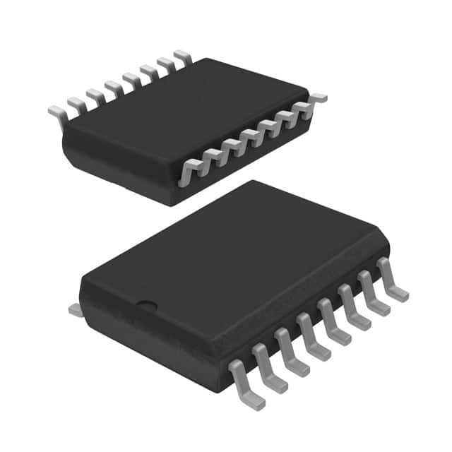
Package
The 74HC7403D,512 is available in a small outline package (SOIC), which provides ease of integration into electronic circuits.
Essence
The essence of this product lies in its ability to perform logical operations and amplify signals efficiently within electronic systems.
Packaging/Quantity
The 74HC7403D,512 is typically packaged in reels or tubes, containing a specific quantity of ICs per package. The exact quantity may vary depending on the manufacturer's specifications.
Specifications
- Supply Voltage: 2V to 6V
- Input Voltage: 0V to VCC
- Output Voltage: 0V to VCC
- Operating Temperature Range: -40°C to +125°C
- Logic Family: HC
- Number of Gates: 4
- Propagation Delay: 10 ns (typical)
Detailed Pin Configuration
The 74HC7403D,512 consists of 14 pins, each serving a specific function:
- Pin 1: Input A1
- Pin 2: Input B1
- Pin 3: Output Y1
- Pin 4: GND (Ground)
- Pin 5: Input A2
- Pin 6: Input B2
- Pin 7: Output Y2
- Pin 8: VCC (Supply Voltage)
- Pin 9: Output Y3
- Pin 10: Input B3
- Pin 11: Input A3
- Pin 12: Output Y4
- Pin 13: Input B4
- Pin 14: Input A4
Functional Features
- Quad 2-input NAND gate functionality
- High-speed operation allows for efficient signal processing
- Low power consumption ensures energy efficiency
- Wide operating voltage range enables compatibility with various systems
- TTL input compatibility facilitates integration with existing circuits
Advantages and Disadvantages
Advantages
- High-speed operation enhances overall system performance
- Low power consumption reduces energy requirements
- Wide operating voltage range provides flexibility in different applications
- Compatibility with TTL inputs simplifies integration into existing circuits
Disadvantages
- Limited number of gates (4) may restrict complex circuit designs
- Propagation delay of 10 ns may impact time-sensitive applications
Working Principles
The 74HC7403D,512 operates based on the principles of digital logic. It utilizes NAND gates to perform logical operations on input signals. The output is determined by the combination of inputs according to the truth table of a NAND gate.
Detailed Application Field Plans
The 74HC7403D,512 finds applications in various fields, including but not limited to: - Digital electronics - Communication systems - Industrial automation - Consumer electronics - Automotive electronics
Detailed and Complete Alternative Models
Some alternative models that offer similar functionality to the 74HC7403D,512 include: - 74LS00 - CD4011 - SN74HC00 - MC14011
These alternative models can be considered based on specific project requirements and availability.
In conclusion, the 74HC7403D,512 is a versatile integrated circuit that offers high-speed operation, low power consumption, and compatibility with TTL inputs. Its quad 2-input NAND gate configuration makes it suitable for various applications in digital electronics, communication systems, and more. While it has limitations in terms of the number of gates and propagation delay, alternative models are available to address specific project needs.
Seznam 10 běžných otázek a odpovědí souvisejících s aplikací 74HC7403D,512 v technických řešeních
Sure! Here are 10 common questions and answers related to the application of 74HC7403D,512 in technical solutions:
Q: What is the function of the 74HC7403D,512? A: The 74HC7403D,512 is a quad 2-input NAND gate with open-drain outputs.
Q: What is an open-drain output? A: An open-drain output can either pull the output low or leave it floating (high impedance state), but it cannot actively drive the output high.
Q: What is the maximum supply voltage for the 74HC7403D,512? A: The maximum supply voltage is 6V.
Q: Can the 74HC7403D,512 be used with both CMOS and TTL logic levels? A: Yes, the 74HC7403D,512 is compatible with both CMOS and TTL logic levels.
Q: What is the typical propagation delay of the 74HC7403D,512? A: The typical propagation delay is around 9 ns.
Q: Can the 74HC7403D,512 be used as a buffer? A: No, the 74HC7403D,512 is specifically designed as a NAND gate and not suitable for use as a buffer.
Q: How many inputs does each NAND gate in the 74HC7403D,512 have? A: Each NAND gate has two inputs.
Q: What is the maximum output current that the 74HC7403D,512 can sink? A: The maximum output current that the 74HC7403D,512 can sink is 25 mA.
Q: Can the 74HC7403D,512 be used in high-speed applications? A: Yes, the 74HC7403D,512 is designed for high-speed operation and can be used in such applications.
Q: Is the 74HC7403D,512 available in different package types? A: Yes, the 74HC7403D,512 is available in various package types, including SOIC, TSSOP, and DIP.
Please note that these answers are general and may vary depending on the specific datasheet and manufacturer's specifications for the 74HC7403D,512.