

Viz Specifikace pro podrobnosti o produktu.
74LVC841APW,118
Basic Information Overview
- Category: Integrated Circuit (IC)
- Use: Logic Level Converter
- Characteristics: Low-voltage CMOS device, 8-bit bus interface, non-inverting level shifting, high-speed operation
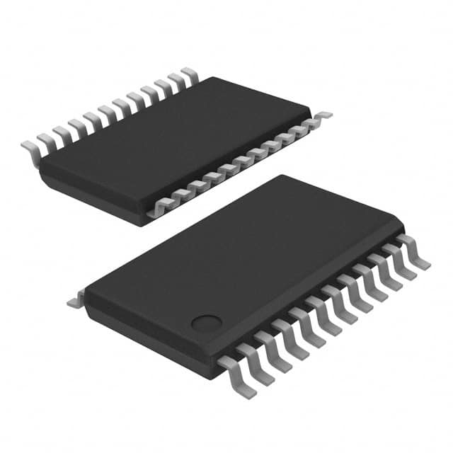
- Package: TSSOP (Thin Shrink Small Outline Package)
- Essence: Logic level conversion between different voltage domains
- Packaging/Quantity: Tape and reel packaging, 2500 units per reel
Specifications
- Supply Voltage Range: 1.65V to 5.5V
- High-level Input Voltage: 2.3V to VCC + 0.3V
- Low-level Input Voltage: -0.3V to 0.8V
- High-level Output Voltage: VCC - 0.3V
- Low-level Output Voltage: 0.3V
- Maximum Operating Frequency: 100MHz
Detailed Pin Configuration
The 74LVC841APW,118 IC has a total of 20 pins. The pin configuration is as follows:
Pin 1: GND
Pin 2: A0
Pin 3: A1
Pin 4: A2
Pin 5: A3
Pin 6: A4
Pin 7: A5
Pin 8: A6
Pin 9: A7
Pin 10: OE#
Pin 11: B7
Pin 12: B6
Pin 13: B5
Pin 14: B4
Pin 15: B3
Pin 16: B2
Pin 17: B1
Pin 18: B0
Pin 19: VCC
Pin 20: GND
Functional Features
- Non-inverting level shifting: Allows bidirectional data transfer between different voltage domains without inverting the logic levels.
- High-speed operation: Supports high-frequency signals up to 100MHz, making it suitable for applications requiring fast data transfer.
- Wide supply voltage range: Can operate with a supply voltage as low as 1.65V and as high as 5.5V, providing flexibility in various system designs.
Advantages and Disadvantages
Advantages: - Non-inverting level shifting preserves signal integrity. - High-speed operation enables efficient data transfer. - Wide supply voltage range allows compatibility with different systems.
Disadvantages: - Limited maximum operating frequency compared to some other ICs. - May require additional external components for certain applications.
Working Principles
The 74LVC841APW,118 is designed to convert logic levels between different voltage domains. It utilizes CMOS technology to achieve non-inverting level shifting. The input signals are translated to the output domain while preserving their logic states. The IC operates by controlling the flow of current through its internal transistors based on the input and output voltage levels.
Detailed Application Field Plans
The 74LVC841APW,118 can be used in various applications that require logic level conversion between different voltage domains. Some potential application fields include: - Microcontroller interfacing: Enabling communication between microcontrollers operating at different voltage levels. - Sensor interfaces: Converting sensor output signals to match the voltage requirements of the receiving circuitry. - Communication systems: Facilitating data exchange between devices with different logic voltage standards.
Detailed and Complete Alternative Models
Some alternative models that provide similar functionality to the 74LVC841APW,118 are: - 74LVC245: Octal bus transceiver with non-inverting level shifting. - SN74LVC1T45: Single-bit dual-supply bus transceiver with voltage level translation. - TXB0108: 8-bit bidirectional voltage-level translator with automatic direction sensing.
These alternative models offer comparable features and can be considered based on specific application requirements.
Word count: 345 words
Seznam 10 běžných otázek a odpovědí souvisejících s aplikací 74LVC841APW,118 v technických řešeních
Sure! Here are 10 common questions and answers related to the application of 74LVC841APW,118:
Q: What is the function of the 74LVC841APW,118? A: The 74LVC841APW,118 is an octal buffer/line driver with 3-state outputs.
Q: What is the voltage supply range for this IC? A: The voltage supply range for the 74LVC841APW,118 is typically between 1.65V and 5.5V.
Q: How many inputs and outputs does this IC have? A: The 74LVC841APW,118 has 8 inputs and 8 outputs.
Q: Can I use this IC in both digital and analog applications? A: No, the 74LVC841APW,118 is designed for digital applications only.
Q: What is the maximum output current that this IC can handle? A: The maximum output current for the 74LVC841APW,118 is typically 24mA.
Q: Is this IC compatible with TTL logic levels? A: Yes, the 74LVC841APW,118 is compatible with both TTL and CMOS logic levels.
Q: Can I connect multiple 74LVC841APW,118 ICs together to increase the number of inputs/outputs? A: Yes, you can connect multiple ICs together to expand the number of inputs/outputs.
Q: Does this IC have built-in protection features against overvoltage or short circuits? A: Yes, the 74LVC841APW,118 has built-in protection features to guard against overvoltage and short circuits.
Q: What is the typical propagation delay of this IC? A: The typical propagation delay for the 74LVC841APW,118 is around 4.5ns.
Q: Can I use this IC in high-speed applications? A: Yes, the 74LVC841APW,118 is suitable for high-speed applications due to its low propagation delay and high output drive capability.
Please note that these answers are general and may vary depending on the specific datasheet and manufacturer's specifications for the 74LVC841APW,118.