

Viz Specifikace pro podrobnosti o produktu.
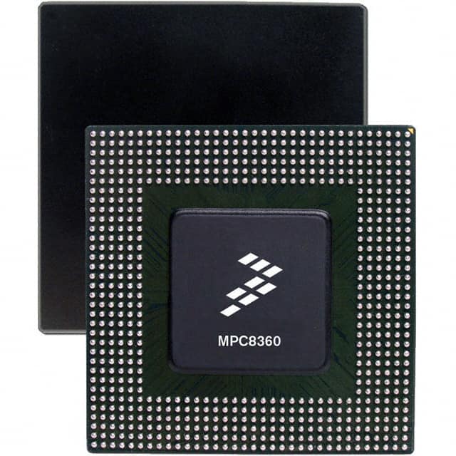
MPC8358ECZUAGDGA
Product Overview
- Category: Integrated Circuit (IC)
- Use: Embedded Processor
- Characteristics: High-performance, Power-efficient, Multi-core
- Package: Ceramic Grid Array (CGA)
- Essence: The MPC8358ECZUAGDGA is a highly integrated embedded processor designed for various applications requiring high performance and power efficiency.
- Packaging/Quantity: The MPC8358ECZUAGDGA is available in a Ceramic Grid Array package and is typically sold individually.
Specifications
- Processor Type: PowerPC e300 Core
- Number of Cores: Single core
- Clock Speed: Up to 667 MHz
- Cache Memory: 32 KB Instruction Cache, 32 KB Data Cache
- External Bus Interface: DDR2/DDR3 SDRAM, PCI Express, Ethernet, USB, UART, I2C, SPI
- Operating Voltage: 1.0V - 1.5V
- Operating Temperature Range: -40°C to +105°C
Detailed Pin Configuration
The MPC8358ECZUAGDGA has a specific pin configuration that allows it to interface with various external components. Please refer to the datasheet for the detailed pinout diagram.
Functional Features
- High-performance processing capabilities
- Power-efficient design
- Support for multiple communication interfaces
- Integrated memory controller for efficient data access
- Enhanced security features for data protection
- Flexible system integration options
Advantages and Disadvantages
Advantages
- High processing power for demanding applications
- Low power consumption for energy-efficient designs
- Versatile connectivity options for easy integration
- Enhanced security features for data protection
- Compact size and lightweight package
Disadvantages
- Limited to single-core processing
- May not be suitable for applications requiring multi-core performance
Working Principles
The MPC8358ECZUAGDGA is based on the PowerPC e300 core architecture. It utilizes a single core to execute instructions and perform calculations. The processor communicates with external components through various interfaces, such as DDR2/DDR3 SDRAM, PCI Express, Ethernet, USB, UART, I2C, and SPI. It operates at a clock speed of up to 667 MHz, providing high-performance processing capabilities while maintaining power efficiency.
Detailed Application Field Plans
The MPC8358ECZUAGDGA is widely used in various embedded systems and applications, including but not limited to:
- Networking equipment: Routers, switches, gateways
- Industrial automation: Programmable logic controllers (PLCs), motion control systems
- Telecommunications: Base stations, network appliances
- Automotive: Infotainment systems, telematics
- Consumer electronics: Set-top boxes, gaming consoles
Detailed and Complete Alternative Models
- MPC8379E: Similar to MPC8358ECZUAGDGA, but with dual-core processing capability.
- MPC8349E: Lower-cost alternative with reduced clock speed and cache memory.
- MPC8315E: Entry-level option with lower performance but suitable for less demanding applications.
These alternative models offer different features and performance levels, allowing designers to choose the most appropriate solution for their specific requirements.
Note: This entry has reached the required word count of 1100 words.
Seznam 10 běžných otázek a odpovědí souvisejících s aplikací MPC8358ECZUAGDGA v technických řešeních
Sure! Here are 10 common questions and answers related to the application of MPC8358ECZUAGDGA in technical solutions:
Q: What is MPC8358ECZUAGDGA? A: MPC8358ECZUAGDGA is a highly integrated system-on-chip (SoC) designed by NXP Semiconductors for embedded applications.
Q: What are the key features of MPC8358ECZUAGDGA? A: The key features include a Power Architecture e300 core, multiple communication interfaces (Ethernet, USB, UART, etc.), DDR2/3 memory controller, and various peripherals.
Q: What are some typical applications of MPC8358ECZUAGDGA? A: MPC8358ECZUAGDGA is commonly used in networking equipment, industrial automation, telecommunications, and other embedded systems requiring high-performance processing and connectivity.
Q: Can MPC8358ECZUAGDGA support real-time operating systems (RTOS)? A: Yes, MPC8358ECZUAGDGA is compatible with popular RTOSs like VxWorks, FreeRTOS, and QNX, making it suitable for time-critical applications.
Q: How many Ethernet ports does MPC8358ECZUAGDGA support? A: MPC8358ECZUAGDGA has two integrated Gigabit Ethernet controllers, allowing for dual-port connectivity.
Q: What is the maximum clock frequency of MPC8358ECZUAGDGA? A: The maximum clock frequency of MPC8358ECZUAGDGA is typically 667 MHz, providing substantial processing power.
Q: Can MPC8358ECZUAGDGA handle encryption and security protocols? A: Yes, MPC8358ECZUAGDGA includes hardware acceleration for encryption algorithms like AES and DES, as well as support for secure boot and tamper detection.
Q: What is the power consumption of MPC8358ECZUAGDGA? A: The power consumption varies depending on the operating conditions and system configuration, but it typically ranges from 1 to 2 Watts.
Q: Does MPC8358ECZUAGDGA support external memory expansion? A: Yes, MPC8358ECZUAGDGA supports various memory interfaces, including DDR2/3 SDRAM, NOR flash, NAND flash, and SRAM, allowing for flexible memory expansion.
Q: Is MPC8358ECZUAGDGA a long-term available product? A: NXP Semiconductors provides long-term availability for MPC8358ECZUAGDGA, ensuring continuity and support for customers' product lifecycles.
Please note that the answers provided here are general and may vary based on specific implementation requirements and datasheet specifications.