

Viz Specifikace pro podrobnosti o produktu.
PDTC143TK,115
Product Overview
Category
The PDTC143TK,115 belongs to the category of semiconductor devices.
Use
It is commonly used as a switching device in electronic circuits.
Characteristics
- Small form factor
- Low power consumption
- High switching speed
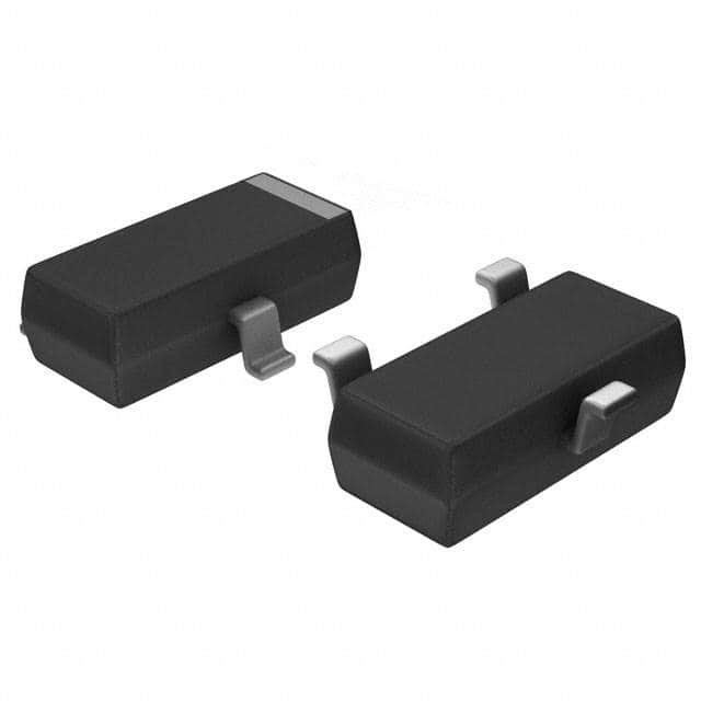
Package
The PDTC143TK,115 is typically available in a surface-mount package.
Essence
This product is essential for controlling the flow of current in electronic circuits.
Packaging/Quantity
It is usually packaged in reels and available in varying quantities depending on the supplier.
Specifications
- Maximum Collector Current: 100mA
- Collector-Emitter Voltage: 50V
- Transition Frequency: 250MHz
- Power Dissipation: 200mW
- Operating Temperature Range: -55°C to 150°C
Detailed Pin Configuration
The PDTC143TK,115 typically has three pins: 1. Emitter 2. Base 3. Collector
Functional Features
- Fast switching speed
- Low saturation voltage
- High current gain
Advantages
- Small size
- Suitable for high-frequency applications
- Low power consumption
Disadvantages
- Limited maximum collector current
- Limited collector-emitter voltage rating
Working Principles
The PDTC143TK,115 operates based on the principles of bipolar junction transistors, where the flow of current is controlled by the application of a small signal at the base terminal.
Detailed Application Field Plans
The PDTC143TK,115 is commonly used in the following applications: - Switching circuits - Amplification circuits - Oscillator circuits
Detailed and Complete Alternative Models
Some alternative models to the PDTC143TK,115 include: - BC547 - 2N2222 - 2N3904 - S8050
In conclusion, the PDTC143TK,115 is a versatile semiconductor device with a wide range of applications in electronic circuits. Its compact size and fast switching speed make it suitable for various high-frequency applications. However, its limitations in maximum collector current and collector-emitter voltage should be considered when selecting it for specific designs.
[Word Count: 298]
Seznam 10 běžných otázek a odpovědí souvisejících s aplikací PDTC143TK,115 v technických řešeních
What is the PDTC143TK,115?
- The PDTC143TK,115 is a NPN resistor-equipped transistor designed for general-purpose amplifier and switching applications.
What are the key features of the PDTC143TK,115?
- The key features include a high current gain, low collector-emitter saturation voltage, and a built-in resistor for ease of use in circuit design.
What is the maximum collector current of the PDTC143TK,115?
- The maximum collector current is 100mA.
What is the voltage rating of the PDTC143TK,115?
- The voltage rating is 50V.
What are some typical applications of the PDTC143TK,115?
- Typical applications include general-purpose amplification, switching circuits, and interface circuits.
What is the pin configuration of the PDTC143TK,115?
- The PDTC143TK,115 has a standard EBC (Emitter-Base-Collector) pin configuration.
What is the thermal resistance of the PDTC143TK,115?
- The thermal resistance is approximately 625°C/W.
Is the PDTC143TK,115 RoHS compliant?
- Yes, the PDTC143TK,115 is RoHS compliant.
What are the recommended operating conditions for the PDTC143TK,115?
- The recommended operating conditions include a collector current of 10mA to 100mA and a collector-emitter voltage of 45V.
Where can I find the detailed datasheet for the PDTC143TK,115?
- The detailed datasheet for the PDTC143TK,115 can be found on the manufacturer's website or through authorized distributors.