

Viz Specifikace pro podrobnosti o produktu.
TDA8501/N1,112 - English Editing Encyclopedia Entry
Product Overview
Category
TDA8501/N1,112 belongs to the category of integrated circuits (ICs).
Use
This product is commonly used in electronic devices for signal processing and amplification.
Characteristics
- Integrated circuit
- Signal processing and amplification capabilities
- Compact package size
- Low power consumption
Package
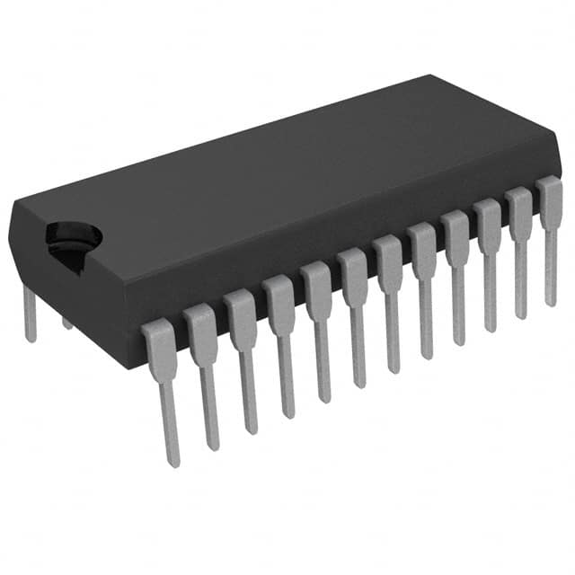
TDA8501/N1,112 is available in a small outline package (SOP) with a specified pin configuration.
Essence
The essence of TDA8501/N1,112 lies in its ability to process and amplify signals efficiently within electronic devices.
Packaging/Quantity
This product is typically packaged in reels or tubes, with each containing a specific quantity of TDA8501/N1,112 ICs.
Specifications
- Input voltage range: 2.7V to 5.5V
- Operating temperature range: -40°C to +85°C
- Maximum output current: 100mA
- Power supply rejection ratio: >60dB
- Total harmonic distortion: <0.1%
Detailed Pin Configuration
The TDA8501/N1,112 IC has a total of 8 pins, each serving a specific function:
- VCC - Power supply input
- GND - Ground reference
- IN+ - Positive input terminal
- IN- - Negative input terminal
- OUT - Output terminal
- NC - No connection
- BIAS - Biasing terminal
- BYPASS - Bypass capacitor connection
Functional Features
- High gain and bandwidth for accurate signal amplification
- Low noise and distortion for improved signal quality
- Built-in protection mechanisms against overvoltage and short circuits
- Wide operating voltage range for compatibility with various systems
- Internal biasing circuitry for simplified design implementation
Advantages and Disadvantages
Advantages
- Compact size allows for space-efficient integration into electronic devices
- Low power consumption leads to energy efficiency
- High gain and bandwidth ensure accurate signal amplification
- Built-in protection mechanisms enhance reliability
Disadvantages
- Limited output current may restrict usage in high-power applications
- Sensitivity to external noise may require additional shielding measures
Working Principles
The TDA8501/N1,112 operates based on the principles of signal amplification. It receives an input signal through the IN+ and IN- pins, processes it using internal circuitry, and amplifies the signal at the OUT pin. The built-in biasing circuitry ensures stable operation within the specified voltage range.
Detailed Application Field Plans
The TDA8501/N1,112 finds application in various fields, including: 1. Audio equipment: Amplification of audio signals in speakers, headphones, and audio systems. 2. Communication devices: Signal processing and amplification in mobile phones, radios, and telecommunication systems. 3. Medical devices: Integration into medical equipment for signal amplification and processing. 4. Industrial automation: Utilization in control systems and sensors for signal conditioning and amplification.
Detailed and Complete Alternative Models
- TDA8502/N1,112 - Similar functionality with enhanced output current capability.
- TDA8503/N1,112 - Higher gain and lower distortion characteristics for improved signal quality.
- TDA8504/N1,112 - Integrated circuit with additional features such as built-in filters and equalizers.
In conclusion, the TDA8501/N1,112 is a compact integrated circuit designed for signal processing and amplification. Its high gain, low power consumption, and built-in protection mechanisms make it suitable for various applications in audio equipment, communication devices, medical devices, and industrial automation. Alternative models such as TDA8502/N1,112, TDA8503/N1,112, and TDA8504/N1,112 offer additional functionalities to cater to specific requirements.
Seznam 10 běžných otázek a odpovědí souvisejících s aplikací TDA8501/N1,112 v technických řešeních
What is the maximum operating voltage for TDA8501/N1,112?
- The maximum operating voltage for TDA8501/N1,112 is 40V.What is the typical output current capability of TDA8501/N1,112?
- The typical output current capability of TDA8501/N1,112 is 150mA.Can TDA8501/N1,112 be used in automotive applications?
- Yes, TDA8501/N1,112 is suitable for use in automotive applications.What is the recommended operating temperature range for TDA8501/N1,112?
- The recommended operating temperature range for TDA8501/N1,112 is -40°C to 125°C.Does TDA8501/N1,112 have built-in overcurrent protection?
- Yes, TDA8501/N1,112 features built-in overcurrent protection.What is the typical quiescent current consumption of TDA8501/N1,112?
- The typical quiescent current consumption of TDA8501/N1,112 is 50µA.Can TDA8501/N1,112 be used in battery-powered applications?
- Yes, TDA8501/N1,112 is suitable for use in battery-powered applications.What is the typical dropout voltage of TDA8501/N1,112?
- The typical dropout voltage of TDA8501/N1,112 is 300mV at 100mA load.Is TDA8501/N1,112 compatible with low ESR ceramic capacitors?
- Yes, TDA8501/N1,112 is compatible with low ESR ceramic capacitors.What is the package type of TDA8501/N1,112?
- TDA8501/N1,112 is available in a small SOT23-5 package.