

Viz Specifikace pro podrobnosti o produktu.
Encyclopedia Entry: 74ACTQ16374SSCX
Product Information Overview
Category: Integrated Circuit (IC)
Use: The 74ACTQ16374SSCX is a high-speed, low-power, 16-bit D-type flip-flop with 3-state outputs. It is designed for use in various digital applications where data storage and transfer are required.
Characteristics: - High-speed operation - Low power consumption - 16-bit data storage capacity - 3-state outputs for bus-oriented applications
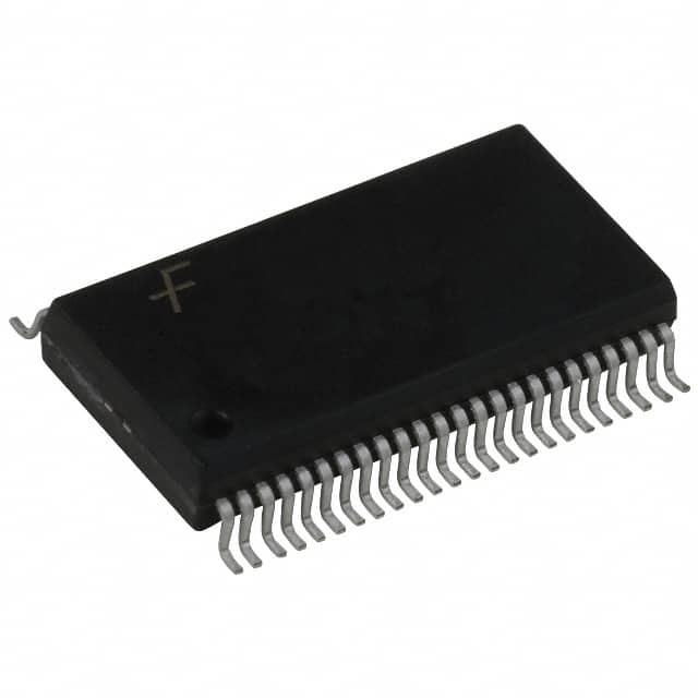
Package: The 74ACTQ16374SSCX is available in a small-outline integrated circuit (SOIC) package. This package provides a compact and reliable solution for integrating the IC into electronic circuits.
Essence: The essence of the 74ACTQ16374SSCX lies in its ability to store and transfer digital data efficiently and reliably. It offers high-speed operation and low power consumption, making it suitable for a wide range of digital applications.
Packaging/Quantity: The 74ACTQ16374SSCX is typically sold in reels or tubes containing multiple units. The exact quantity may vary depending on the supplier and customer requirements.
Specifications
- Supply Voltage Range: 2.0V to 6.0V
- Input Voltage Range: -0.5V to VCC + 0.5V
- Output Voltage Range: -0.5V to VCC + 0.5V
- Operating Temperature Range: -40°C to +85°C
- Maximum Clock Frequency: 200MHz
Detailed Pin Configuration
The 74ACTQ16374SSCX has a total of 48 pins, which are assigned specific functions. Here is the detailed pin configuration:
- Pin 1: Data Input (D0)
- Pin 2: Data Input (D1)
- Pin 3: Data Input (D2)
- Pin 4: Data Input (D3)
- Pin 5: Data Input (D4)
- Pin 6: Data Input (D5)
- Pin 7: Data Input (D6)
- Pin 8: Data Input (D7)
- Pin 9: Data Input (D8)
- Pin 10: Data Input (D9)
- Pin 11: Data Input (D10)
- Pin 12: Data Input (D11)
- Pin 13: Data Input (D12)
- Pin 14: Data Input (D13)
- Pin 15: Data Input (D14)
- Pin 16: Data Input (D15)
- Pin 17: Clock Input (CLK)
- Pin 18: Clock Enable (CLKEN)
- Pin 19: Output Enable (OE)
- Pin 20: Master Reset (MR)
- Pin 21: Q0 Output
- Pin 22: Q1 Output
- Pin 23: Q2 Output
- Pin 24: Q3 Output
- Pin 25: Q4 Output
- Pin 26: Q5 Output
- Pin 27: Q6 Output
- Pin 28: Q7 Output
- Pin 29: Q8 Output
- Pin 30: Q9 Output
- Pin 31: Q10 Output
- Pin 32: Q11 Output
- Pin 33: Q12 Output
- Pin 34: Q13 Output
- Pin 35: Q14 Output
- Pin 36: Q15 Output
- Pin 37: GND (Ground)
- Pin 38: GND (Ground)
- Pin 39: GND (Ground)
- Pin 40: VCC (Power Supply)
- Pin 41: VCC (Power Supply)
- Pin 42: VCC (Power Supply)
- Pin 43: VCC (Power Supply)
- Pin 44: VCC (Power Supply)
- Pin 45: VCC (Power Supply)
- Pin 46: VCC (Power Supply)
- Pin 47: VCC (Power Supply)
- Pin 48: VCC (Power Supply)
Functional Features
The 74ACTQ16374SSCX offers the following functional features:
- Data storage and transfer: The IC can store 16 bits of digital data and transfer it to the output pins.
- Clock enable and output enable control: The CLKEN and OE pins allow for precise control over clocking and output operations.
- Master reset: The MR pin provides a means to reset the flip-flop to its initial state.
- 3-state outputs: The Q0-Q15 outputs can be
Seznam 10 běžných otázek a odpovědí souvisejících s aplikací 74ACTQ16374SSCX v technických řešeních
Sure! Here are 10 common questions and answers related to the application of 74ACTQ16374SSCX in technical solutions:
Question: What is the 74ACTQ16374SSCX?
Answer: The 74ACTQ16374SSCX is a 16-bit D-type flip-flop with 3-state outputs, commonly used in digital circuits.Question: What is the operating voltage range for the 74ACTQ16374SSCX?
Answer: The operating voltage range for this IC is typically between 4.5V and 5.5V.Question: How many flip-flops are there in the 74ACTQ16374SSCX?
Answer: The 74ACTQ16374SSCX contains 16 individual flip-flops.Question: What is the maximum clock frequency supported by the 74ACTQ16374SSCX?
Answer: The maximum clock frequency supported by this IC is typically around 200 MHz.Question: Can I use the 74ACTQ16374SSCX in both synchronous and asynchronous applications?
Answer: Yes, the 74ACTQ16374SSCX can be used in both synchronous and asynchronous applications.Question: What is the purpose of the 3-state outputs in this IC?
Answer: The 3-state outputs allow multiple devices to share a common bus without interfering with each other.Question: What is the power consumption of the 74ACTQ16374SSCX?
Answer: The power consumption of this IC is relatively low, making it suitable for battery-powered applications.Question: Can I cascade multiple 74ACTQ16374SSCX ICs together?
Answer: Yes, you can cascade multiple ICs to increase the number of flip-flops in your circuit.Question: Does the 74ACTQ16374SSCX have any built-in protection features?
Answer: Yes, this IC has built-in protection against electrostatic discharge (ESD) and latch-up.Question: What are some common applications for the 74ACTQ16374SSCX?
Answer: Some common applications include data storage, address decoding, bus interfacing, and general-purpose digital logic circuits.
Please note that the answers provided here are general and may vary depending on specific datasheet specifications and application requirements.