

Viz Specifikace pro podrobnosti o produktu.
74LVTH16240MEA
Basic Information Overview
- Category: Integrated Circuit (IC)
- Use: Buffer/Driver
- Characteristics: High-speed, low-voltage, and low-power consumption
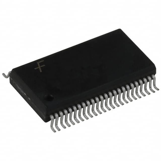
- Package: 48-pin TSSOP (Thin Shrink Small Outline Package)
- Essence: Logic Level Translator
- Packaging/Quantity: Tape and Reel, 2500 units per reel
Specifications
- Supply Voltage Range: 2.7V to 3.6V
- Input Voltage Range: 0V to VCC
- Output Voltage Range: 0V to VCC
- Operating Temperature Range: -40°C to +85°C
- Propagation Delay Time: 4.5ns (typical)
- Output Drive Capability: ±24mA
Detailed Pin Configuration
The 74LVTH16240MEA has a total of 48 pins, which are divided into four groups of twelve pins each. The pin configuration is as follows:
Group A (Pins 1-12)
- Pin 1: Output Y1
- Pin 2: Output Y2
- Pin 3: Output Y3
- Pin 4: Output Y4
- Pin 5: Output Y5
- Pin 6: Output Y6
- Pin 7: Output Y7
- Pin 8: Output Y8
- Pin 9: GND (Ground)
- Pin 10: Output Enable (OE)
- Pin 11: Input B1
- Pin 12: Input B2
Group B (Pins 13-24)
- Pin 13: Output Y9
- Pin 14: Output Y10
- Pin 15: Output Y11
- Pin 16: Output Y12
- Pin 17: Output Y13
- Pin 18: Output Y14
- Pin 19: Output Y15
- Pin 20: Output Y16
- Pin 21: VCC (Supply Voltage)
- Pin 22: Input B3
- Pin 23: Input B4
- Pin 24: Input B5
Group C (Pins 25-36)
- Pin 25: Output Y17
- Pin 26: Output Y18
- Pin 27: Output Y19
- Pin 28: Output Y20
- Pin 29: Output Y21
- Pin 30: Output Y22
- Pin 31: Output Y23
- Pin 32: Output Y24
- Pin 33: GND (Ground)
- Pin 34: Input B6
- Pin 35: Input B7
- Pin 36: Input B8
Group D (Pins 37-48)
- Pin 37: Output Y25
- Pin 38: Output Y26
- Pin 39: Output Y27
- Pin 40: Output Y28
- Pin 41: Output Y29
- Pin 42: Output Y30
- Pin 43: Output Y31
- Pin 44: Output Y32
- Pin 45: VCC (Supply Voltage)
- Pin 46: Input B9
- Pin 47: Input B10
- Pin 48: Input B11
Functional Features
- Logic Level Translation: The 74LVTH16240MEA is designed to translate signals between different logic voltage levels, making it suitable for interfacing between devices operating at different voltage levels.
- High-Speed Operation: With a typical propagation delay time of 4.5ns, this IC ensures fast signal transmission and response times.
- Low-Voltage Operation: It operates within a low voltage range of 2.7V to 3.6V, making it compatible with various low-power applications.
- Output Drive Capability: The IC can drive up to ±24mA of current, enabling it to interface with a wide range of devices.
Advantages and Disadvantages
Advantages
- High-speed operation allows for quick signal transmission.
- Low-voltage operation reduces power consumption.
- Logic level translation enables interfacing between different voltage domains.
- Adequate output drive capability ensures compatibility with various devices.
Disadvantages
- Limited number of input and output pins may restrict the complexity of the circuitry it can handle.
- Not suitable for applications requiring higher voltage levels.
Working Principles
The 74LVTH16240MEA is based on CMOS (Complementary Metal-Oxide-Semiconductor) technology. It utilizes a combination of NMOS (N-channel Metal-Oxide-Semiconductor) and PMOS (P-channel Metal-Oxide-Semiconductor) transistors to achieve logic level translation. When an input signal is applied, the internal circuitry translates it to the desired logic level
Seznam 10 běžných otázek a odpovědí souvisejících s aplikací 74LVTH16240MEA v technických řešeních
Sure! Here are 10 common questions and answers related to the application of 74LVTH16240MEA in technical solutions:
Q: What is the 74LVTH16240MEA? A: The 74LVTH16240MEA is a 16-bit buffer/driver with 3-state outputs, designed for low-voltage (3.3V) applications.
Q: What is the maximum operating frequency of the 74LVTH16240MEA? A: The maximum operating frequency of the 74LVTH16240MEA is typically around 200 MHz.
Q: Can the 74LVTH16240MEA be used as a level shifter? A: Yes, the 74LVTH16240MEA can be used as a level shifter to convert signals between different voltage levels.
Q: What is the output current capability of the 74LVTH16240MEA? A: The 74LVTH16240MEA has a typical output current capability of ±32 mA.
Q: Can the 74LVTH16240MEA be used in bidirectional data transfer applications? A: No, the 74LVTH16240MEA is a unidirectional buffer/driver and does not support bidirectional data transfer.
Q: What is the power supply voltage range for the 74LVTH16240MEA? A: The 74LVTH16240MEA operates within a power supply voltage range of 2.7V to 3.6V.
Q: Does the 74LVTH16240MEA have built-in ESD protection? A: Yes, the 74LVTH16240MEA has built-in ESD protection on all inputs and outputs.
Q: Can the 74LVTH16240MEA be used in high-speed data communication applications? A: Yes, the 74LVTH16240MEA is suitable for high-speed data communication applications due to its low propagation delay.
Q: What is the typical input capacitance of the 74LVTH16240MEA? A: The typical input capacitance of the 74LVTH16240MEA is around 3 pF.
Q: Is the 74LVTH16240MEA compatible with other logic families? A: Yes, the 74LVTH16240MEA is compatible with both TTL and CMOS logic families, making it versatile for various applications.
Please note that these answers are general and may vary depending on specific datasheet specifications and application requirements.