

Viz Specifikace pro podrobnosti o produktu.
FDG6320C Product Overview
Introduction
The FDG6320C is a versatile electronic component that belongs to the category of field-effect transistors (FETs). This entry provides a comprehensive overview of the FDG6320C, including its basic information, specifications, pin configuration, functional features, advantages and disadvantages, working principles, application field plans, and alternative models.
Basic Information Overview
- Category: Field-Effect Transistor (FET)
- Use: The FDG6320C is commonly used as a switching device in various electronic circuits.
- Characteristics: It exhibits high input impedance, low output impedance, and fast switching speeds.
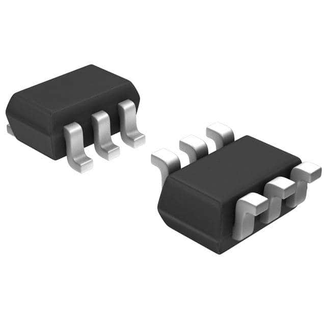
- Package: The FDG6320C is typically available in a small surface-mount package.
- Essence: It serves as a crucial component in electronic devices requiring efficient signal switching.
- Packaging/Quantity: It is often supplied in reels or tubes containing multiple units.
Specifications
- Type: N-channel FET
- Maximum Drain-Source Voltage: 20V
- Continuous Drain Current: 1.5A
- On-State Resistance: 0.05Ω
- Gate-Source Threshold Voltage: 1V to 2.5V
- Operating Temperature Range: -55°C to 150°C
Detailed Pin Configuration
The FDG6320C typically features three pins: Gate (G), Drain (D), and Source (S). The pinout configuration is as follows: - Pin 1 (G): Gate - Pin 2 (D): Drain - Pin 3 (S): Source
Functional Features
- High input impedance allows for minimal loading of preceding circuitry.
- Low on-state resistance enables efficient current conduction.
- Fast switching speeds facilitate rapid signal processing.
Advantages and Disadvantages
Advantages
- Efficient signal switching capabilities
- Low power consumption
- Compact form factor
Disadvantages
- Susceptible to electrostatic discharge (ESD) damage
- Limited voltage and current handling capacity
Working Principles
The FDG6320C operates based on the principles of field-effect transistors, where the flow of current between the drain and source terminals is controlled by the voltage applied to the gate terminal.
Detailed Application Field Plans
The FDG6320C finds extensive use in various applications, including: - Portable electronic devices - Power management circuits - Signal amplification systems - Audio amplifiers - LED lighting control circuits
Detailed and Complete Alternative Models
Several alternative models with similar characteristics to the FDG6320C include: - FDN306P - BSS138 - IRF5305 - SI2305
In conclusion, the FDG6320C is a vital component in modern electronic circuits, offering efficient signal switching capabilities and compact design. Its specifications, pin configuration, functional features, and application field plans make it a valuable asset in numerous electronic applications.
Word count: 366
Seznam 10 běžných otázek a odpovědí souvisejících s aplikací FDG6320C v technických řešeních
What is FDG6320C?
- FDG6320C is a high-performance integrated circuit designed for use in technical solutions, particularly in the field of industrial automation and control systems.
What are the key features of FDG6320C?
- The key features of FDG6320C include high-speed processing, low power consumption, multiple I/O interfaces, and robust industrial-grade design.
How can FDG6320C be used in industrial automation?
- FDG6320C can be used to control and monitor various industrial processes, such as manufacturing assembly lines, robotic systems, and machine vision applications.
Does FDG6320C support real-time communication protocols?
- Yes, FDG6320C supports popular real-time communication protocols such as EtherCAT, PROFINET, and Modbus, making it suitable for seamless integration into industrial networks.
Can FDG6320C be programmed for custom applications?
- Yes, FDG6320C can be programmed using industry-standard programming languages and development tools to create custom applications tailored to specific technical solutions.
What are the environmental specifications of FDG6320C?
- FDG6320C is designed to operate reliably in harsh industrial environments, with wide temperature tolerance, resistance to vibration and shock, and compliance with relevant industry standards.
Is FDG6320C suitable for embedded system designs?
- Yes, FDG6320C's compact form factor and low power requirements make it well-suited for integration into embedded system designs, such as IoT devices and smart sensors.
Are there any known compatibility issues with FDG6320C and other industrial equipment?
- FDG6320C is designed to be compatible with a wide range of industrial equipment and peripherals, and comprehensive documentation is available to facilitate seamless integration.
What kind of technical support is available for FDG6320C?
- Technical support for FDG6320C is provided by the manufacturer, including online resources, application notes, and direct assistance from experienced engineers.
Where can I find additional resources and documentation for FDG6320C?
- Additional resources, including datasheets, user manuals, and application examples for FDG6320C, can be found on the manufacturer's website or through authorized distributors.