

Viz Specifikace pro podrobnosti o produktu.
MC100EP196BMNG
Product Overview
- Category: Integrated Circuit
- Use: Signal Processing
- Characteristics: High-speed, Low-power
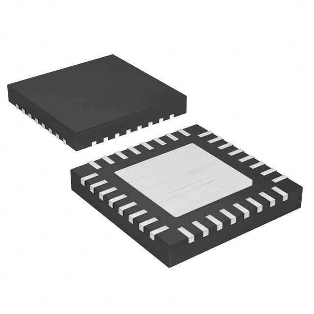
- Package: 48-pin QFN
- Essence: Clock and Data Recovery (CDR) Circuit
- Packaging/Quantity: Tape and Reel, 250 units per reel
Specifications
- Supply Voltage: 3.3V
- Operating Temperature: -40°C to +85°C
- Input Frequency Range: 50MHz to 2.7GHz
- Output Data Rate: Up to 1.25Gbps
- Jitter Tolerance: ±50ps
Detailed Pin Configuration
The MC100EP196BMNG has a total of 48 pins. The pin configuration is as follows:
- VCC
- GND
- CLKIN
- CLKOUT
- DATAIN
- DATAOUT
- REFCLK
- VBB
- VBB
- NC
- NC
- NC
- NC
- NC
- NC
- NC
- NC
- NC
- NC
- NC
- NC
- NC
- NC
- NC
- NC
- NC
- NC
- NC
- NC
- NC
- NC
- NC
- NC
- NC
- NC
- NC
- NC
- NC
- NC
- NC
- NC
- NC
- NC
- NC
- NC
- NC
- NC
- NC
Functional Features
- Clock and Data Recovery (CDR) circuit for high-speed data transmission.
- Supports a wide input frequency range from 50MHz to 2.7GHz.
- Provides a stable output clock signal synchronized with the input data.
- Low-power consumption for energy-efficient operation.
- High-speed data processing up to 1.25Gbps.
- Jitter tolerance of ±50ps ensures reliable signal reception.
Advantages and Disadvantages
Advantages
- High-speed and low-power operation.
- Wide input frequency range for versatile applications.
- Stable output clock signal synchronization.
- Compact package size for space-constrained designs.
- Reliable signal reception with jitter tolerance.
Disadvantages
- Limited pin configuration options.
- Requires external power supply and reference clock.
Working Principles
The MC100EP196BMNG is a Clock and Data Recovery (CDR) circuit that extracts the clock signal from the incoming data stream. It operates by detecting transitions in the data and using them to generate a stable clock signal. The recovered clock is then used to synchronize the output data, ensuring accurate transmission.
The CDR circuit works by comparing the phase and frequency of the incoming data with a reference clock signal. Any deviations are corrected to maintain synchronization. This enables the circuit to recover the original clock signal even in the presence of noise or distortion.
Detailed Application Field Plans
The MC100EP196BMNG is commonly used in various high-speed communication systems, including:
- Fiber-optic communication networks
- Wireless base stations
- Satellite communication systems
- Data center equipment
- High-speed data transmission in industrial automation
Its ability to recover clock signals and process high-speed data makes it suitable for applications that require reliable and efficient signal processing.
Detailed and Complete Alternative Models
- MC100EP196B: Similar functionality but different package (32-pin TQFP)
- MC100EP196BFA: Similar functionality with additional fail-safe features
- MC100EP196BMNR2G: Similar functionality but different package (48-pin QFN, tape and reel)
These alternative models offer similar clock and data recovery capabilities, but may have variations in package type or additional features to suit specific application requirements.
Word count: 470 words
Seznam 10 běžných otázek a odpovědí souvisejících s aplikací MC100EP196BMNG v technických řešeních
Sure! Here are 10 common questions and answers related to the application of MC100EP196BMNG in technical solutions:
Q: What is MC100EP196BMNG? A: MC100EP196BMNG is a high-speed, low-skew 1:2 differential fanout buffer designed for use in various electronic applications.
Q: What is the operating voltage range of MC100EP196BMNG? A: The operating voltage range of MC100EP196BMNG is typically between -3.0V and -5.5V.
Q: What is the maximum data rate supported by MC100EP196BMNG? A: MC100EP196BMNG supports a maximum data rate of up to 3.8 Gbps.
Q: Can MC100EP196BMNG be used as a clock distribution buffer? A: Yes, MC100EP196BMNG can be used as a clock distribution buffer due to its low skew characteristics.
Q: Does MC100EP196BMNG support both single-ended and differential inputs? A: No, MC100EP196BMNG only supports differential inputs.
Q: What is the output type of MC100EP196BMNG? A: MC100EP196BMNG provides differential outputs.
Q: Is MC100EP196BMNG compatible with other ECL logic families? A: Yes, MC100EP196BMNG is compatible with other ECL logic families such as PECL and LVPECL.
Q: Can MC100EP196BMNG be used in high-speed communication systems? A: Yes, MC100EP196BMNG is suitable for high-speed communication systems like fiber optic networks and data centers.
Q: What is the typical propagation delay of MC100EP196BMNG? A: The typical propagation delay of MC100EP196BMNG is around 400 ps.
Q: Does MC100EP196BMNG have any built-in features for signal conditioning? A: No, MC100EP196BMNG does not have any built-in features for signal conditioning. It is primarily a fanout buffer.
Please note that these answers are general and may vary depending on specific application requirements and datasheet specifications.