

Viz Specifikace pro podrobnosti o produktu.
MC14551BF
Product Overview
- Category: Integrated Circuit
- Use: Digital Multiplexer/Demultiplexer
- Characteristics: High-speed, low-power consumption
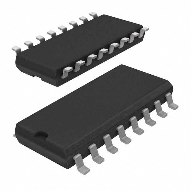
- Package: 16-pin DIP (Dual In-line Package)
- Essence: MC14551BF is a digital multiplexer/demultiplexer IC that allows for the selection of one out of multiple input signals and routing it to a single output line.
- Packaging/Quantity: Available in tubes or reels, with 25 pieces per tube/reel.
Specifications
- Supply Voltage: 3V to 18V
- Input Voltage: 0V to Vcc
- Output Voltage: 0V to Vcc
- Operating Temperature Range: -40°C to +85°C
- Propagation Delay Time: 250ns (max)
- Power Dissipation: 500mW (max)
Pin Configuration
The MC14551BF has a total of 16 pins, which are assigned specific functions. The pin configuration is as follows:
- A0: Address Input 0
- A1: Address Input 1
- A2: Address Input 2
- E: Enable Input
- I0: Data Input 0
- I1: Data Input 1
- I2: Data Input 2
- I3: Data Input 3
- I4: Data Input 4
- I5: Data Input 5
- I6: Data Input 6
- I7: Data Input 7
- O: Output
- GND: Ground
- Vcc: Supply Voltage
- NC: No Connection
Functional Features
- Digital multiplexing and demultiplexing functionality
- Wide supply voltage range for flexibility
- Low power consumption for energy efficiency
- High-speed operation for quick signal routing
- Easy integration into digital circuit designs
Advantages and Disadvantages
Advantages
- Versatile multiplexing/demultiplexing capabilities
- Wide operating voltage range allows for compatibility with various systems
- Low power consumption helps conserve energy
- High-speed operation enables efficient signal routing
Disadvantages
- Limited number of input/output lines (8 in this case)
- Propagation delay may affect real-time applications
- Requires additional external components for complete functionality
Working Principles
The MC14551BF operates based on the principles of digital multiplexing and demultiplexing. It uses the address inputs (A0, A1, A2) to select one of the data inputs (I0-I7) and routes it to the output pin (O). The enable input (E) controls the operation of the IC.
When a specific combination of address inputs is applied, the corresponding data input is selected and passed through to the output. This allows for the consolidation of multiple signals into a single line or the distribution of a single signal to multiple lines.
Application Field Plans
The MC14551BF finds applications in various fields where digital multiplexing and demultiplexing are required. Some potential application areas include:
- Communication Systems: Multiplexing multiple data streams onto a single transmission line.
- Data Acquisition: Selecting and routing analog signals from multiple sensors to an ADC (Analog-to-Digital Converter).
- Digital Displays: Controlling the display of different information on a shared screen.
- Industrial Automation: Managing multiple control signals in automated systems.
- Audio/Video Switching: Routing audio/video signals to different output devices.
Alternative Models
There are several alternative models available that offer similar functionality to the MC14551BF. Some popular alternatives include:
- CD4051B: 8-channel analog multiplexer/demultiplexer IC.
- SN74HC151: 8-input digital multiplexer IC.
- 74HC138: 3-to-8 line decoder/demultiplexer IC.
These alternative models can be considered based on specific requirements and compatibility with the overall system design.
In conclusion, the MC14551BF is a versatile digital multiplexer/demultiplexer IC that offers high-speed operation, low power consumption, and wide supply voltage range. It finds applications in various fields such as communication systems, data acquisition, digital displays, industrial automation, and audio/video switching. While it has some limitations, there are alternative models available to suit different needs.
Seznam 10 běžných otázek a odpovědí souvisejících s aplikací MC14551BF v technických řešeních
Sure! Here are 10 common questions and answers related to the application of MC14551BF in technical solutions:
Q: What is MC14551BF? A: MC14551BF is a CMOS integrated circuit that consists of multiple 8-bit shift registers with input/output latches and control circuitry.
Q: What are the typical applications of MC14551BF? A: MC14551BF is commonly used in various technical solutions such as data storage, serial-to-parallel conversion, parallel-to-serial conversion, and general-purpose digital logic applications.
Q: How many shift registers are present in MC14551BF? A: MC14551BF contains eight independent 8-bit shift registers.
Q: What is the maximum clock frequency supported by MC14551BF? A: The maximum clock frequency supported by MC14551BF is typically around 5 MHz.
Q: Can MC14551BF be cascaded to increase the number of shift registers? A: Yes, MC14551BF can be cascaded to increase the number of shift registers by connecting the output of one IC to the input of another.
Q: What is the power supply voltage range for MC14551BF? A: MC14551BF operates within a power supply voltage range of 3V to 18V.
Q: Does MC14551BF support both serial and parallel data transfer? A: Yes, MC14551BF supports both serial and parallel data transfer modes depending on the configuration of its control pins.
Q: Can MC14551BF be used for bidirectional data transfer? A: No, MC14551BF is primarily designed for unidirectional data transfer.
Q: Are there any special considerations for interfacing MC14551BF with microcontrollers? A: When interfacing MC14551BF with microcontrollers, it is important to ensure proper voltage level compatibility and use appropriate level shifters if necessary.
Q: Are there any recommended decoupling capacitors for MC14551BF? A: It is generally recommended to include decoupling capacitors (e.g., 0.1μF ceramic capacitors) near the power supply pins of MC14551BF to minimize noise and stabilize the operation.
Please note that these questions and answers are general in nature and may vary depending on specific application requirements and circuit design considerations.