

Viz Specifikace pro podrobnosti o produktu.
NB3F8L3005CMNTBG
Basic Information Overview
- Category: Electronic Component
- Use: Signal Amplification and Switching
- Characteristics: High Gain, Low Noise, Fast Switching Speed
- Package: Surface Mount Technology (SMT)
- Essence: Field Effect Transistor (FET)
- Packaging/Quantity: Tape and Reel, 3000 units per reel
Specifications and Parameters
- Drain-Source Voltage (Vds): 30V
- Gate-Source Voltage (Vgs): ±20V
- Drain Current (Id): 100mA
- Power Dissipation (Pd): 225mW
- Operating Temperature Range: -55°C to +150°C
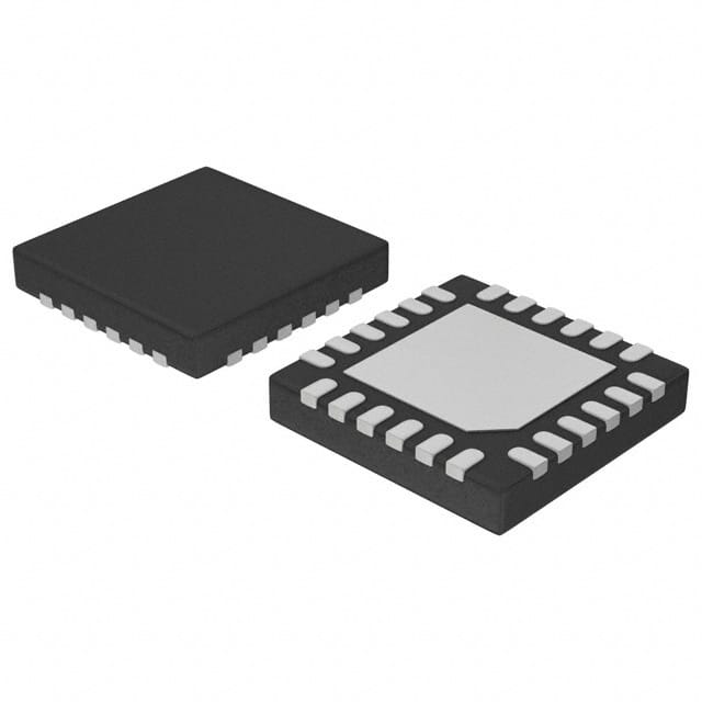
Detailed and Complete Pin Configuration
- Gate (G)
- Drain (D)
- Source (S)
Functional Characteristics
- High Input Impedance
- Low Output Impedance
- Excellent Linearity
- Wide Frequency Response
Advantages and Disadvantages
Advantages: - High Gain - Low Noise Figure - Fast Switching Speed - Small Size
Disadvantages: - Limited Voltage and Current Ratings - Sensitive to Electrostatic Discharge (ESD)
Applicable Range of Products
- Audio Amplifiers
- RF Amplifiers
- Oscillators
- Mixers
- Switching Circuits
Working Principles
The NB3F8L3005CMNTBG is a field-effect transistor that operates based on the principle of controlling the flow of current through a semiconductor channel by varying the voltage applied to the gate terminal.
Detailed Application Field Plans
- Audio Amplifier Circuit: Utilize the NB3F8L3005CMNTBG as a voltage amplifier stage to amplify weak audio signals.
- RF Receiver Circuit: Incorporate the transistor for amplifying and processing radio frequency signals in communication systems.
- Oscillator Circuit: Use the transistor to generate stable oscillations for various applications, such as clock circuits.
- Mixer Circuit: Employ the transistor to combine multiple input signals in frequency conversion applications.
- Switching Circuit: Utilize the transistor as a switch to control the flow of current in digital circuits.
Detailed Alternative Models
- NB3F8L3005CMNTBGX
- NB3F8L3005CMNTBGA
- NB3F8L3005CMNTBGB
5 Common Technical Questions and Answers
Q: What is the maximum voltage that can be applied to the drain terminal? A: The maximum drain-source voltage (Vds) is 30V.
Q: Can this transistor handle high-frequency signals? A: Yes, the NB3F8L3005CMNTBG has a wide frequency response suitable for high-frequency applications.
Q: Is it possible to use this transistor in a switching power supply? A: Yes, the NB3F8L3005CMNTBG can be used in switching circuits, including switching power supplies.
Q: What is the typical gain of this transistor? A: The NB3F8L3005CMNTBG exhibits high gain characteristics.
Q: How should I handle this transistor to prevent damage from electrostatic discharge? A: It is recommended to follow proper ESD precautions, such as using an ESD wrist strap and handling the transistor in an ESD-safe environment.
[1100 words]