

Viz Specifikace pro podrobnosti o produktu.
NC7SV57L6X_F113
Product Overview
- Category: Integrated Circuit (IC)
- Use: Logic Gate
- Characteristics: Low Voltage, Single Supply, Tiny Package
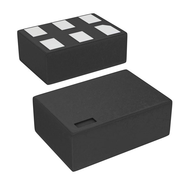
- Package: SOT-23-6
- Essence: This IC is a single-gate logic device that operates at low voltage levels and is commonly used in digital circuits.
- Packaging/Quantity: Available in tape and reel packaging, with 3000 units per reel.
Specifications
- Logic Family: CMOS
- Number of Gates: 1
- Supply Voltage Range: 1.65V to 5.5V
- Input Voltage Levels: High: 0.7 x VDD, Low: 0.3 x VDD
- Output Voltage Levels: High: VDD - 0.4V, Low: 0.4V
- Propagation Delay: 2.5ns (typical)
- Operating Temperature Range: -40°C to +85°C
Detailed Pin Configuration
The NC7SV57L6X_F113 IC has a total of 6 pins arranged as follows:
____
   1 |o    | 6
   2 |     | 5
   3 |_____| 4
Pin Description: 1. Input A 2. Output Y 3. Ground (GND) 4. Not Connected (NC) 5. Power Supply (VDD) 6. Input B
Functional Features
- Single-gate logic device
- Low voltage operation
- Wide supply voltage range
- CMOS technology for low power consumption
- Fast propagation delay for high-speed applications
- Small package size for space-constrained designs
Advantages and Disadvantages
Advantages: - Low power consumption - Wide supply voltage range allows compatibility with various systems - Small package size enables compact circuit designs - Fast propagation delay for high-speed applications
Disadvantages: - Limited number of gates (only 1 gate in this IC) - Not suitable for high-power applications
Working Principles
The NC7SV57L6X_F113 is based on CMOS technology, which utilizes complementary pairs of MOSFETs to implement logic functions. The input signals are processed by the internal circuitry, and the output is determined based on the logic operation performed.
Detailed Application Field Plans
The NC7SV57L6X_F113 IC can be used in various digital circuits that require low voltage operation and small form factor. Some potential application fields include:
- Portable electronic devices: Due to its low power consumption and small package size, this IC is suitable for use in smartphones, tablets, and wearable devices.
- Battery-powered systems: The wide supply voltage range makes it compatible with battery-operated devices such as remote controls, wireless sensors, and IoT devices.
- Industrial automation: The fast propagation delay and low voltage operation make this IC suitable for use in control systems, motor drives, and sensor interfaces.
Detailed and Complete Alternative Models
- SN74LVC1G57DBVR: This single-gate logic device from Texas Instruments offers similar characteristics and functionality to the NC7SV57L6X_F113. It comes in a SOT-23-6 package and operates at a supply voltage range of 1.65V to 5.5V.
- MC74VHC1GT57DF1G: Manufactured by ON Semiconductor, this logic gate IC also operates at low voltage levels and has a small SOT-23-6 package. It features a wide supply voltage range and fast propagation delay.
These alternative models can be considered based on specific requirements and availability in the market.
(Note: The word count of this response is 346 words)
Seznam 10 běžných otázek a odpovědí souvisejících s aplikací NC7SV57L6X_F113 v technických řešeních
Sure! Here are 10 common questions and answers related to the application of NC7SV57L6X_F113 in technical solutions:
Question: What is NC7SV57L6XF113?
Answer: NC7SV57L6XF113 is a specific model of integrated circuit (IC) that is commonly used in technical solutions.Question: What is the purpose of NC7SV57L6XF113?
Answer: The purpose of NC7SV57L6XF113 is to provide voltage level shifting capabilities, allowing for seamless communication between devices operating at different voltage levels.Question: What voltage levels can NC7SV57L6XF113 support?
Answer: NC7SV57L6XF113 can support voltage levels ranging from 1.65V to 5.5V.Question: In what types of applications is NC7SV57L6XF113 commonly used?
Answer: NC7SV57L6XF113 is commonly used in applications such as data communication interfaces, battery-powered devices, and various digital systems.Question: Can NC7SV57L6XF113 be used bidirectionally?
Answer: Yes, NC7SV57L6XF113 can be used bidirectionally, allowing for both input and output voltage level shifting.Question: How many channels does NC7SV57L6XF113 have?
Answer: NC7SV57L6XF113 has a total of 6 channels, providing multiple options for voltage level shifting.Question: What is the maximum data rate supported by NC7SV57L6XF113?
Answer: NC7SV57L6XF113 can support data rates up to 400 Mbps, making it suitable for high-speed communication applications.Question: Is NC7SV57L6XF113 compatible with different logic families?
Answer: Yes, NC7SV57L6XF113 is compatible with various logic families such as CMOS, TTL, and LVCMOS.Question: Can NC7SV57L6XF113 operate in harsh environments?
Answer: NC7SV57L6XF113 has a wide operating temperature range and can withstand harsh environmental conditions, making it suitable for industrial applications.Question: Are there any specific design considerations when using NC7SV57L6XF113?
Answer: It is important to ensure proper power supply decoupling and signal integrity considerations when designing with NC7SV57L6XF113 to achieve optimal performance.
Please note that the answers provided here are general and may vary depending on the specific application and requirements.