

Viz Specifikace pro podrobnosti o produktu.
NC7SVL08FHX
Basic Information Overview
- Category: Integrated Circuit (IC)
- Use: Logic Gate
- Characteristics: Low Voltage, High-Speed, Tiny Package
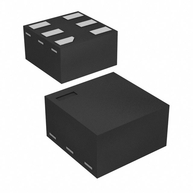
- Package: SOT-23-5
- Essence: AND Gate
- Packaging/Quantity: Tape and Reel, 3000 pieces per reel
Specifications
- Supply Voltage Range: 1.65V to 5.5V
- Input Voltage Range: 0V to VCC
- Output Voltage Range: 0V to VCC
- Operating Temperature Range: -40°C to +85°C
- Propagation Delay: 2.5ns (typical)
Detailed Pin Configuration
The NC7SVL08FHX has a total of 5 pins arranged in the following configuration: 1. Pin 1: Input A 2. Pin 2: Input B 3. Pin 3: Ground (GND) 4. Pin 4: Output Y 5. Pin 5: Power Supply (VCC)
Functional Features
- Performs logical AND operation on two input signals (A and B)
- Provides a single output signal (Y) based on the logical operation result
- Supports low voltage operation, making it suitable for battery-powered devices
- Offers high-speed performance, enabling quick response times in digital circuits
- Compact package size allows for space-efficient designs
Advantages and Disadvantages
Advantages: - Low power consumption - Wide supply voltage range - Small form factor - Fast propagation delay
Disadvantages: - Limited number of inputs (only two) - Not suitable for high-power applications
Working Principles
The NC7SVL08FHX is an AND gate, which means it performs the logical AND operation on its two input signals (A and B). The output (Y) is high (logic 1) only when both inputs are high; otherwise, the output is low (logic 0). This gate operates on a supply voltage ranging from 1.65V to 5.5V and provides a fast propagation delay of approximately 2.5ns.
Detailed Application Field Plans
The NC7SVL08FHX can be used in various applications that require logical AND operations, such as: - Digital signal processing - Data communication systems - Microcontrollers and microprocessors - Battery-powered devices - Sensor networks
Detailed and Complete Alternative Models
- SN74LVC1G08DBVR: Single 2-Input Positive-AND Gate, SOT-23-5 package
- MC74VHC1G08DTT1G: Single 2-Input AND Gate, SOT-23-5 package
- CD4081BE: Quad 2-Input AND Gate, DIP-14 package
- 74HC08N: Quad 2-Input AND Gate, DIP-14 package
- HEF4081BP: Quad 2-Input AND Gate, DIP-14 package
(Note: The above list includes alternative models with different package types and/or multiple gates.)
In conclusion, the NC7SVL08FHX is a low-voltage, high-speed AND gate integrated circuit. It offers compact size, low power consumption, and wide supply voltage range. Its fast propagation delay makes it suitable for various digital applications. However, it has limited input capacity and is not recommended for high-power scenarios. Alternative models with similar functionality are available in different package options.
Seznam 10 běžných otázek a odpovědí souvisejících s aplikací NC7SVL08FHX v technických řešeních
Sure! Here are 10 common questions and answers related to the application of NC7SVL08FHX in technical solutions:
Question: What is the NC7SVL08FHX?
Answer: The NC7SVL08FHX is a low-voltage, single-gate, 2-input AND gate integrated circuit.Question: What is the operating voltage range of the NC7SVL08FHX?
Answer: The NC7SVL08FHX operates within a voltage range of 0.9V to 3.6V.Question: Can the NC7SVL08FHX be used in battery-powered devices?
Answer: Yes, the low operating voltage range makes it suitable for use in battery-powered devices.Question: What is the maximum output current of the NC7SVL08FHX?
Answer: The NC7SVL08FHX has a maximum output current of 32mA.Question: Can the NC7SVL08FHX be used in high-speed applications?
Answer: Yes, the NC7SVL08FHX has a propagation delay of only 2.5ns, making it suitable for high-speed applications.Question: Is the NC7SVL08FHX compatible with other logic families?
Answer: Yes, the NC7SVL08FHX is compatible with both CMOS and TTL logic families.Question: Can I use the NC7SVL08FHX in automotive applications?
Answer: Yes, the NC7SVL08FHX is AEC-Q100 qualified, making it suitable for automotive applications.Question: Does the NC7SVL08FHX have built-in ESD protection?
Answer: Yes, the NC7SVL08FHX has built-in ESD protection up to 2kV.Question: Can I use the NC7SVL08FHX in industrial control systems?
Answer: Yes, the NC7SVL08FHX is suitable for use in industrial control systems due to its wide operating temperature range (-40°C to +85°C).Question: Is the NC7SVL08FHX available in different package options?
Answer: Yes, the NC7SVL08FHX is available in various package options, including SOT-23 and SC70.
Please note that these answers are general and may vary depending on the specific application and requirements.