

Viz Specifikace pro podrobnosti o produktu.
NC7WZ04L6X_F113
Basic Information Overview
- Category: Integrated Circuit (IC)
- Use: Logic Gate Inverter
- Characteristics: Low-power, high-speed, small form factor
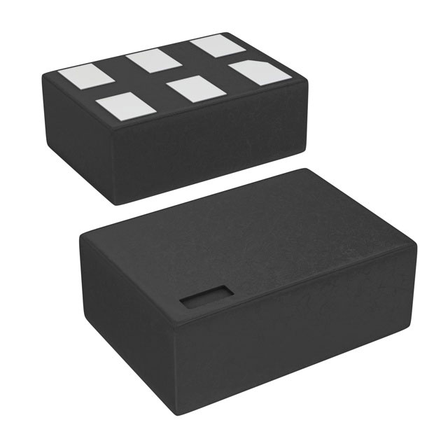
- Package: SOT-363
- Essence: Complementary Metal-Oxide-Semiconductor (CMOS) technology
- Packaging/Quantity: Tape and Reel, 3000 units per reel
Specifications
- Supply Voltage Range: 1.65V to 5.5V
- Input Voltage Range: 0V to VCC
- Output Voltage Range: 0V to VCC
- Maximum Operating Frequency: 200 MHz
- Propagation Delay: 2.5 ns (typical)
Detailed Pin Configuration
The NC7WZ04L6X_F113 IC has a total of six pins: 1. GND (Ground) 2. A (Input) 3. Y (Output) 4. B (Input) 5. VCC (Power supply) 6. NC (No Connection)
Functional Features
- Logic Inversion: The NC7WZ04L6X_F113 is a single inverter gate that performs logical inversion on the input signal.
- High-Speed Operation: It operates at a maximum frequency of 200 MHz, making it suitable for high-speed applications.
- Low Power Consumption: This IC is designed to consume minimal power, making it ideal for battery-powered devices.
- Small Form Factor: The SOT-363 package ensures a compact size, enabling integration into space-constrained designs.
Advantages and Disadvantages
Advantages: - Low power consumption extends battery life in portable devices. - High-speed operation enables efficient data processing. - Small form factor allows for integration in compact designs.
Disadvantages: - Limited voltage range may restrict compatibility with certain systems. - Lack of built-in protection features may require additional circuitry for robustness.
Working Principles
The NC7WZ04L6X_F113 is based on CMOS technology, which utilizes both NMOS and PMOS transistors to achieve logic functions. In the case of this IC, a single NMOS transistor acts as a pull-down switch, while a single PMOS transistor acts as a pull-up switch. When the input signal is low, the NMOS transistor conducts, pulling the output signal high. Conversely, when the input signal is high, the PMOS transistor conducts, pulling the output signal low. This behavior results in logical inversion.
Detailed Application Field Plans
The NC7WZ04L6X_F113 is commonly used in various applications, including: 1. Battery-Powered Devices: Its low power consumption makes it suitable for use in portable electronics such as smartphones, tablets, and wearables. 2. Communication Systems: It can be employed in signal processing circuits, data transmission systems, and networking equipment. 3. Industrial Control Systems: The IC finds application in control units, sensors, and actuators used in automation and robotics. 4. Automotive Electronics: It can be utilized in automotive control modules, infotainment systems, and driver assistance systems.
Detailed and Complete Alternative Models
- SN74LVC1G04DBVR: Single Inverter Gate, SOT-23 package, 1.65V to 5.5V supply voltage range.
- MC74VHC1G04DFT1G: Single Inverter Gate, SOT-353 package, 2V to 5.5V supply voltage range.
- TC7SZ04FU(T5L,F): Single Inverter Gate, SOT-353 package, 1.65V to 5.5V supply voltage range.
(Note: These alternative models are provided as examples and may have different specifications and characteristics. It is recommended to refer to the respective datasheets for detailed information.)
In conclusion, the NC7WZ04L6X_F113 is a low-power, high-speed logic gate inverter IC that finds application in various electronic systems. Its small form factor, low power consumption, and high-speed operation make it a versatile choice for numerous applications.
Seznam 10 běžných otázek a odpovědí souvisejících s aplikací NC7WZ04L6X_F113 v technických řešeních
Sure! Here are 10 common questions and answers related to the application of NC7WZ04L6X_F113 in technical solutions:
Question: What is NC7WZ04L6XF113?
Answer: NC7WZ04L6XF113 is a specific model of a logic gate integrated circuit (IC) that consists of six inverters.Question: What is the purpose of using NC7WZ04L6XF113 in technical solutions?
Answer: NC7WZ04L6XF113 is commonly used for signal inversion, level shifting, and buffering in various electronic circuits.Question: Can NC7WZ04L6XF113 be used in both digital and analog circuits?
Answer: No, NC7WZ04L6XF113 is specifically designed for digital circuits and is not suitable for analog applications.Question: What is the voltage range supported by NC7WZ04L6XF113?
Answer: NC7WZ04L6XF113 operates within a voltage range of 1.65V to 5.5V, making it compatible with a wide range of digital systems.Question: How many inputs and outputs does NC7WZ04L6XF113 have?
Answer: NC7WZ04L6XF113 has six inputs and six corresponding outputs, allowing for multiple signal inversions simultaneously.Question: Can NC7WZ04L6XF113 handle high-speed signals?
Answer: Yes, NC7WZ04L6XF113 is designed to operate at high speeds, making it suitable for applications requiring fast signal processing.Question: Is NC7WZ04L6XF113 available in different package options?
Answer: Yes, NC7WZ04L6XF113 is available in various package options, such as SOT-23 and SC70, providing flexibility for different circuit designs.Question: Can NC7WZ04L6XF113 be used in battery-powered devices?
Answer: Yes, NC7WZ04L6XF113 has a low power consumption and can be used in battery-powered devices to minimize energy usage.Question: Are there any specific precautions to consider when using NC7WZ04L6XF113?
Answer: It is important to ensure that the voltage levels applied to the inputs of NC7WZ04L6XF113 are within the specified range to prevent damage.Question: Can NC7WZ04L6XF113 be cascaded with other logic gates?
Answer: Yes, NC7WZ04L6XF113 can be cascaded with other logic gates to create more complex digital circuits and perform advanced functions.
Please note that these questions and answers are general and may vary depending on the specific application and requirements.