

Viz Specifikace pro podrobnosti o produktu.
NL17SZ14XV5T2G
Basic Information Overview
- Category: Integrated Circuit (IC)
- Use: Logic Gate
- Characteristics: High-speed, low-power consumption
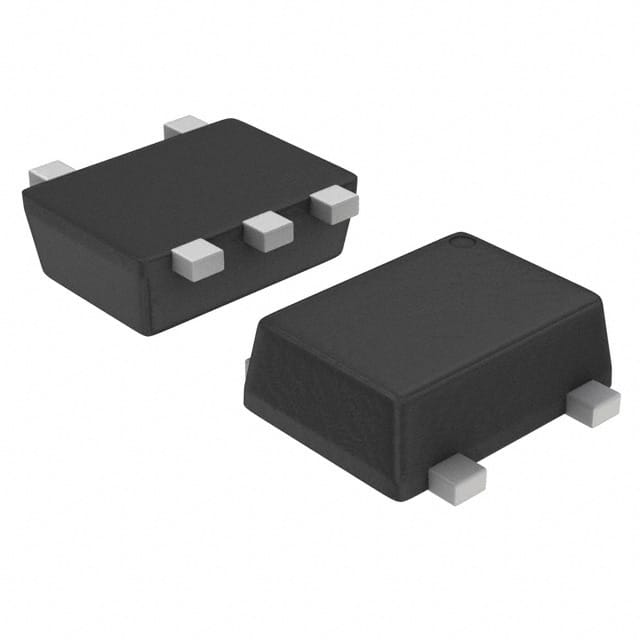
- Package: SOT-353 (SC-88A)
- Essence: Single Schmitt-Trigger Inverter
- Packaging/Quantity: Tape and Reel / 3000 units per reel
Specifications
- Supply Voltage Range: 1.65V to 5.5V
- Input Voltage Range: 0V to VCC
- Output Voltage Range: 0V to VCC
- Maximum Operating Frequency: 200 MHz
- Propagation Delay Time: 3.8 ns (typical)
- Quiescent Current: 0.9 µA (typical)
Detailed Pin Configuration
The NL17SZ14XV5T2G has a total of 5 pins: 1. GND (Ground): Connected to the ground reference potential. 2. IN (Input): Accepts the input signal to be inverted. 3. OUT (Output): Provides the inverted output signal. 4. VCC (Power Supply): Connected to the positive supply voltage. 5. NC (No Connection): This pin is not internally connected and can be left unconnected.
Functional Features
- Schmitt-Trigger Input: The NL17SZ14XV5T2G incorporates a Schmitt-trigger input, allowing it to provide hysteresis and improve noise immunity.
- High-Speed Operation: With a maximum operating frequency of 200 MHz, this IC enables fast signal processing.
- Low Power Consumption: The quiescent current of only 0.9 µA makes it suitable for battery-powered applications.
- Wide Voltage Range: The NL17SZ14XV5T2G can operate within a wide supply voltage range from 1.65V to 5.5V.
Advantages and Disadvantages
Advantages: - High-speed operation enables efficient signal processing. - Low power consumption prolongs battery life in portable devices. - Wide voltage range allows compatibility with various systems.
Disadvantages: - Limited number of pins restricts the complexity of circuits that can be built using this IC. - Lack of internal connection on one pin may require additional care during circuit design.
Working Principles
The NL17SZ14XV5T2G is a single Schmitt-trigger inverter, which means it takes an input signal and produces its inverted form at the output. The Schmitt-trigger input provides hysteresis, ensuring a clean and stable output even in the presence of noise or signal fluctuations. This IC operates by amplifying and inverting the input signal based on the defined threshold levels.
Detailed Application Field Plans
The NL17SZ14XV5T2G finds applications in various fields, including: 1. Digital Communication Systems: Used for signal conditioning and level shifting in high-speed data transmission. 2. Consumer Electronics: Integrated into audio/video equipment, smartphones, and tablets for signal processing and logic control. 3. Industrial Automation: Employed in control systems, sensors, and actuators for reliable signal conversion and interfacing. 4. Automotive Electronics: Utilized in vehicle control units, infotainment systems, and driver assistance modules for logic operations.
Detailed and Complete Alternative Models
- SN74LVC1G14DBVR: Single Schmitt-Trigger Inverter with similar specifications and package (SOT-23).
- MC74VHC1GT14DF1G: Single Schmitt-Trigger Inverter with extended temperature range and smaller package (SOT-563).
- TC7SZ14FU(T5L,F): Single Schmitt-Trigger Inverter with enhanced ESD protection and smaller package (USV).
Note: The above alternative models are just a few examples, and there are several other options available in the market.
This entry provides comprehensive information about the NL17SZ14XV5T2G, including its product details, specifications, pin configuration, functional features, advantages, disadvantages, working principles, application field plans, and alternative models.
Seznam 10 běžných otázek a odpovědí souvisejících s aplikací NL17SZ14XV5T2G v technických řešeních
Sure! Here are 10 common questions and answers related to the application of NL17SZ14XV5T2G in technical solutions:
Q: What is NL17SZ14XV5T2G? A: NL17SZ14XV5T2G is a specific type of logic gate, specifically an inverter, used in digital circuits.
Q: What is the function of NL17SZ14XV5T2G in technical solutions? A: NL17SZ14XV5T2G is used to invert the logical state of a signal, converting a high voltage level to a low voltage level and vice versa.
Q: How can NL17SZ14XV5T2G be used in technical solutions? A: NL17SZ14XV5T2G can be used in various applications such as signal conditioning, level shifting, clock synchronization, and data transmission.
Q: What are the key features of NL17SZ14XV5T2G? A: Some key features of NL17SZ14XV5T2G include low power consumption, small package size, wide operating voltage range, and compatibility with different logic families.
Q: What is the voltage range supported by NL17SZ14XV5T2G? A: NL17SZ14XV5T2G typically supports a wide voltage range, often ranging from 1.65V to 5.5V.
Q: Can NL17SZ14XV5T2G be used in both analog and digital circuits? A: No, NL17SZ14XV5T2G is specifically designed for digital circuits and is not suitable for analog applications.
Q: Is NL17SZ14XV5T2G compatible with other logic families? A: Yes, NL17SZ14XV5T2G is compatible with various logic families such as CMOS, TTL, and LVCMOS.
Q: What is the maximum operating frequency of NL17SZ14XV5T2G? A: The maximum operating frequency of NL17SZ14XV5T2G typically ranges from tens of megahertz to hundreds of megahertz.
Q: Can NL17SZ14XV5T2G be used in high-speed data transmission applications? A: Yes, NL17SZ14XV5T2G can be used in high-speed data transmission applications, but its performance may vary depending on the specific requirements.
Q: Where can I find more information about NL17SZ14XV5T2G and its application in technical solutions? A: You can refer to the datasheet provided by the manufacturer or visit their official website for detailed information on NL17SZ14XV5T2G and its application notes.