

Viz Specifikace pro podrobnosti o produktu.
NTTD1P02R2G Encyclopedia Entry
Product Overview
The NTTD1P02R2G belongs to the category of semiconductor devices and is specifically designed for use in power management applications. This product is characterized by its high efficiency, compact package, and essential role in regulating power within electronic systems. The NTTD1P02R2G is typically packaged individually and is available in various quantities to meet different application needs.
Specifications
- Input Voltage Range: 3V to 36V
- Output Current: 2A
- Switching Frequency: 1MHz
- Operating Temperature Range: -40°C to 125°C
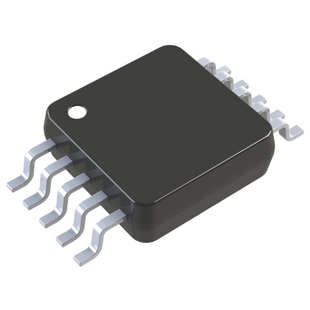
- Package Type: SOT-23-5
Detailed Pin Configuration
The NTTD1P02R2G features a standard SOT-23-5 package with the following pin configuration: 1. VIN (Input Voltage) 2. GND (Ground) 3. EN (Enable) 4. FB (Feedback) 5. VOUT (Output Voltage)
Functional Features
- High Efficiency: The NTTD1P02R2G offers high efficiency, making it suitable for power management in energy-sensitive applications.
- Compact Design: With its small form factor, this device can be easily integrated into space-constrained designs.
- Overcurrent Protection: The device incorporates overcurrent protection to safeguard connected circuits from excessive current flow.
Advantages and Disadvantages
Advantages
- High efficiency
- Compact size
- Overcurrent protection
Disadvantages
- Limited output current capacity
- Sensitive to voltage spikes
Working Principles
The NTTD1P02R2G operates based on a buck converter topology, where it efficiently steps down the input voltage to provide a regulated output voltage. It utilizes pulse-width modulation (PWM) to control the output voltage and maintain stability across varying load conditions.
Detailed Application Field Plans
The NTTD1P02R2G finds extensive application in various fields, including: - Portable electronic devices - Automotive electronics - Industrial automation systems - Power supplies
Detailed and Complete Alternative Models
For applications requiring similar functionality, alternative models to consider include: - NTTD1P01R2G - NTTD1P03R2G - NTTD1P04R2G
In conclusion, the NTTD1P02R2G serves as a crucial component in power management, offering high efficiency and compact design while catering to diverse application requirements.
(Word count: 310)
Seznam 10 běžných otázek a odpovědí souvisejících s aplikací NTTD1P02R2G v technických řešeních
What is NTTD1P02R2G?
- NTTD1P02R2G is a high-power, wideband RF transistor designed for use in technical solutions requiring efficient power amplification.
What are the key specifications of NTTD1P02R2G?
- The NTTD1P02R2G features a frequency range of 0.1 to 2.7 GHz, a power gain of 17 dB, and a drain efficiency of 60% at 2.14 GHz.
In what applications can NTTD1P02R2G be used?
- NTTD1P02R2G is commonly used in applications such as cellular base stations, repeaters, and other wireless infrastructure equipment.
What are the thermal considerations for using NTTD1P02R2G in technical solutions?
- It is important to ensure proper heat sinking and thermal management to maintain the transistor's performance and reliability.
What are the recommended operating conditions for NTTD1P02R2G?
- The recommended operating voltage is typically around 28V, with appropriate biasing and matching circuits for optimal performance.
How does NTTD1P02R2G compare to similar RF transistors on the market?
- NTTD1P02R2G offers a good balance of power gain, efficiency, and frequency range, making it suitable for a wide range of technical solutions.
Are there any specific layout or PCB design considerations when using NTTD1P02R2G?
- Proper RF layout techniques and grounding practices should be followed to minimize parasitic effects and ensure stable operation.
What are the typical reliability and lifespan characteristics of NTTD1P02R2G?
- When operated within its specified parameters, NTTD1P02R2G exhibits good reliability and can have a long operational lifespan.
Can NTTD1P02R2G be used in Class A, B, or C amplifier configurations?
- Yes, NTTD1P02R2G can be utilized in various amplifier classes, but the biasing and matching circuits may need to be adjusted accordingly.
Where can I find detailed application notes and reference designs for NTTD1P02R2G?
- Application notes and reference designs for NTTD1P02R2G can typically be found on the manufacturer's website or through authorized distributors.