

Viz Specifikace pro podrobnosti o produktu.
R1LV0408DSB-5SI#B0
Product Overview
Category: Integrated Circuit (IC)
Use: Memory device
Characteristics: - High-speed operation - Low power consumption - Large storage capacity - Reliable performance
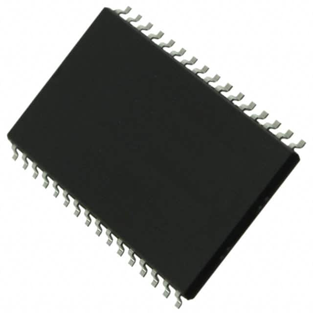
Package: Small Outline Integrated Circuit (SOIC)
Essence: Non-volatile memory chip
Packaging/Quantity: Each package contains one R1LV0408DSB-5SI#B0 chip.
Specifications
- Memory Type: Flash memory
- Organization: 4M words x 8 bits
- Supply Voltage: 2.7V - 3.6V
- Access Time: 70 ns
- Operating Temperature Range: -40°C to +85°C
- Package Dimensions: 150 mil (width) x 209 mil (length)
- Pin Count: 32
Detailed Pin Configuration
The R1LV0408DSB-5SI#B0 chip has a total of 32 pins, which are assigned specific functions as follows:
| Pin Number | Function | |------------|----------| | 1 | VCC | | 2 | A0 | | 3 | A1 | | 4 | A2 | | 5 | A3 | | 6 | A4 | | 7 | A5 | | 8 | A6 | | 9 | A7 | | 10 | A8 | | 11 | A9 | | 12 | A10 | | 13 | A11 | | 14 | A12 | | 15 | A13 | | 16 | A14 | | 17 | A15 | | 18 | A16 | | 19 | A17 | | 20 | A18 | | 21 | A19 | | 22 | A20 | | 23 | CE# | | 24 | WE# | | 25 | OE# | | 26 | I/O0 | | 27 | I/O1 | | 28 | I/O2 | | 29 | I/O3 | | 30 | GND | | 31 | NC | | 32 | VCCQ |
Functional Features
- High-speed read and write operations
- Low power consumption in standby mode
- Automatic sleep mode for power saving
- Built-in error correction code (ECC) for data integrity
- Block erase and sector erase functions
- Write protection feature for data security
Advantages and Disadvantages
Advantages: - Fast access time - Large storage capacity - Low power consumption - Reliable performance - Error correction capability
Disadvantages: - Limited endurance (limited number of erase/write cycles) - Relatively high cost compared to other memory technologies
Working Principles
The R1LV0408DSB-5SI#B0 is a flash memory chip that stores data electronically. It utilizes floating-gate transistors to trap electrical charges, representing binary information as "0" or "1". The stored data remains intact even when the power supply is disconnected.
During read operations, the chip retrieves the stored data by sensing the voltage levels on the memory cells. Write operations involve applying higher voltages to the selected memory cells to either store new data or erase existing data.
Detailed Application Field Plans
The R1LV0408DSB-5SI#B0 chip finds applications in various electronic devices, including but not limited to: - Personal computers - Laptops - Mobile phones - Digital cameras - Gaming consoles - Automotive electronics - Industrial control systems
Detailed and Complete Alternative Models
- R1LV0408DSB-7SI#B0: Similar to R1LV0408DSB-5SI#B0, but with a faster access time of 70 ns.
- R1LV0408DSB-10SI#B0: Similar to R1LV0408DSB-5SI#B0, but with a slower access time of 100 ns.
- R1LV0408DSB-5SI#B1: Similar to R1LV0408DSB-5SI#B0, but with an extended operating temperature range (-40°C to +105°C).
These alternative models provide options based on specific requirements such as speed, temperature range, and compatibility.
Word count: 511 words
Seznam 10 běžných otázek a odpovědí souvisejících s aplikací R1LV0408DSB-5SI#B0 v technických řešeních
Sure! Here are 10 common questions and answers related to the application of R1LV0408DSB-5SI#B0 in technical solutions:
Q1: What is R1LV0408DSB-5SI#B0? A1: R1LV0408DSB-5SI#B0 is a specific model of dynamic random-access memory (DRAM) chip used for storing and retrieving digital information in electronic devices.
Q2: What is the capacity of R1LV0408DSB-5SI#B0? A2: R1LV0408DSB-5SI#B0 has a capacity of 4 megabits (Mb), which is equivalent to 512 kilobytes (KB).
Q3: What is the operating voltage range for R1LV0408DSB-5SI#B0? A3: The operating voltage range for R1LV0408DSB-5SI#B0 is typically between 2.7V and 3.6V.
Q4: What is the speed rating of R1LV0408DSB-5SI#B0? A4: R1LV0408DSB-5SI#B0 has a speed rating of 5 nanoseconds (ns), indicating the time it takes to access data stored in the memory.
Q5: What interface does R1LV0408DSB-5SI#B0 use? A5: R1LV0408DSB-5SI#B0 uses a parallel interface, specifically an 8-bit wide data bus.
Q6: Can R1LV0408DSB-5SI#B0 be used in battery-powered devices? A6: Yes, R1LV0408DSB-5SI#B0 can be used in battery-powered devices as it operates within the typical voltage range of such devices.
Q7: Is R1LV0408DSB-5SI#B0 compatible with common microcontrollers? A7: Yes, R1LV0408DSB-5SI#B0 is compatible with many common microcontrollers that support parallel memory interfaces.
Q8: Can R1LV0408DSB-5SI#B0 be used for real-time applications? A8: Yes, R1LV0408DSB-5SI#B0 can be used for real-time applications as it has a relatively fast access time of 5 ns.
Q9: What is the temperature range for reliable operation of R1LV0408DSB-5SI#B0? A9: R1LV0408DSB-5SI#B0 is designed to operate reliably within a temperature range of -40°C to +85°C.
Q10: Are there any specific precautions to consider when using R1LV0408DSB-5SI#B0? A10: It is recommended to follow the manufacturer's datasheet and guidelines for proper handling, storage, and electrical connections to ensure optimal performance and reliability of R1LV0408DSB-5SI#B0.